The Circuit Board Design workbench is displayed.
-
Select the xy plane.
The Sketcher workbench is launched .
. -
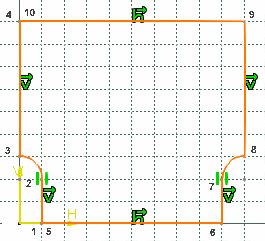
Sketch the contour of the Board.
To do so: - start the sketch from 1 and go to 4,
- stop at 4 by double-clicking,
- start again from 5 and go to 10,
- stop at 10 by double-clicking.
Before you click to start and stop, a blue symbol
 must appear to illustrate coincidence between the start and end
points, to get a closed contour.
must appear to illustrate coincidence between the start and end
points, to get a closed contour.
Refer to the Sketcher Getting Started.The profile looks like this:
-
Quit the Sketcher using Exit Sketcher
 :
:
You are back in the Circuit Board Design workbench .
. -
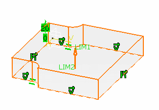
The Pad Definition dialog box appears. 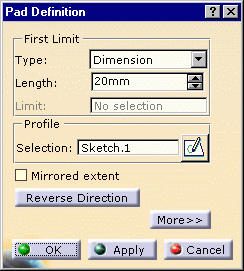
-
Enter 2mm in Length.
-
Click OK.
The pad turns green, which means the board has been created.
The board has been created from the active part: Part1(BOARD).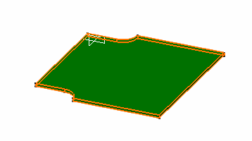
CATIA recognizes the first pad created as the board.