|
SVGA Adapters With Cirrus GD542x
CL5428 SVGA /A
Adapter ID 917A 
P/N 84G7001, EC No. D43621, FRU 84G7001.
Silk marked as " IGH0879BA SVGA CARD, IBI, M4V0".
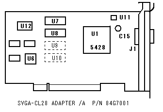 |
U1
CL-GD5428-80QC-A
U6
PALCE22V10H ( dated 3/4/94 )
U7,8 SOJ DRAM
TC514260BJ-70 *1
U9,10 Solder pads for
additional VRAM
U12 84G7129
M5M27C256AFP ( BIOS ? )
U11 LM334
C15 Capacitor
( 10/25A/40B )
J1
Video Connector
*1 For SOJ DRAM chips, See below
|
Originally equipped in 5521-YSB/YWB. Not available as an OBI.
This
adapter is Flicker Free.
Ready to upgrade to 2MB
( but you need soldering work ). Just solder SOJ DRAM chips
at the solder pads.
Each pin # 14 of solder pads for additional VRAMs are already
connected to pin # 141 of CL5428 through 100 ohms
resistor which is marked "R26".
Value printed atop of the resistor is "101". Reply Video
Board uses 33 ohms resistor
for
this connection.
Click here
for Adapter BIOS ROM.
Win9x built-in driver can detect 2MB and provide 1024 x768 16bit mode
( if the system property is correct ). NT4
can detect only 1MB of VRAM even if you have 2MB installed.
SOJ Chips ;
Following chips are used for CL SVGA adapters.
Micron MT4C16257DJ-6
NEC 42S4260-70
Toshiba TC514260BJ-70
Hitachi HM514260DJ-6
OKI
M514260ASL-70J
and more...See bottom
of this section.
|
Layout around GD5428 and
LM334 ( PLease compare with Server
SVGA CL5428 )
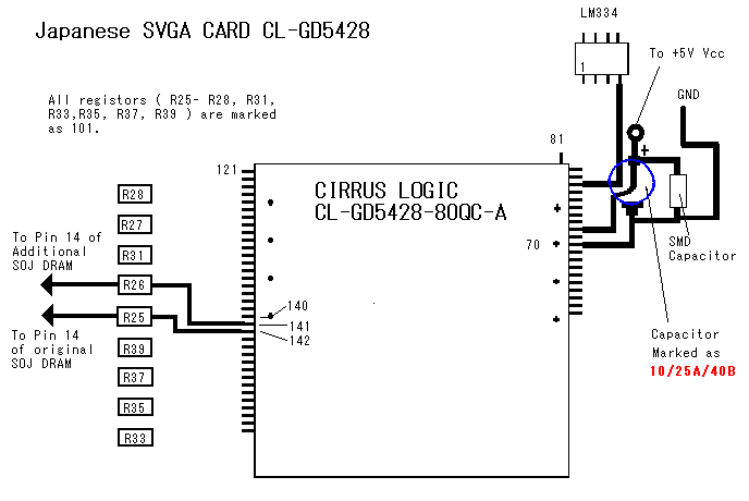
@917A.ADF
.... Really simple . Isn't it?
---------------------------------------------------------------------------
AdapterId 0917AH
AdapterName "SVGA CL-28 Adapte /A"
NumBytes 1
FixedResources
pos[0]=XXXXXXXXb
mem 0c0000h-0c7fffh
------------------------------------------------------------------------------
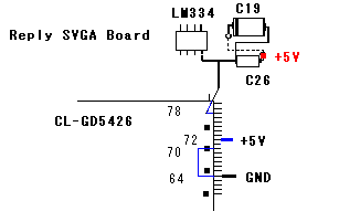
Reply Video
Board ( CL-GD5426 ) (
pumped up to 2MB )
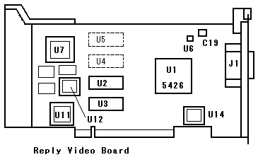 |
U1
CL-GD5426-80QC-A
U2, 3 SOJ DRAM
MT41167257DJ-6 ( on mine )
U4, 5 Solder pads for
additional VRAM
U6 LM334
C19 Capacitor
336/16K/221
U7
BIOS
U11 PALCE22
U12 PALCE16V
U14 GAL
16V8B
J1
Video Connector |
For detailed information, Click here
for Ardent Toll, mirrored by Tim Clark .
Drivers for DOS/Win3.1 are available at Bob
Eager's page.
Win9x/NT have builtin drivers.
Win9x builtin driver can detect 2MB and provide 1024 x768 16bit
mode ( if the system property is correct ).
NT4 can detect only 1MB of VRAM even if additional 1MB have been
installed.
Layout Around GD5426 and LM334
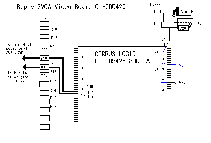
@8182.ADF REPLY CL26
---------------------------------------------------------------------
AdapterId 08182H
AdapterName "REPLY VIDEO ADAPTER"
NumBytes 1
NamedItem
Prompt "CARD ENABLE"
choice "card enable" pos[0]=XXXXxxx1b
mem 0c0000h-0c7fffh
Help
"Call tech support"
--------------------------------------------------------------------
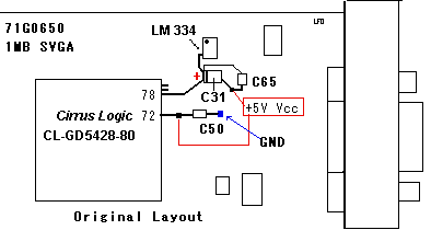
1MB SVGA Adapter CL-GD5428
FRU P/N 71G0650, P/N 06H6917 With Delivery Boys
marking. Adapter ID is 917B.
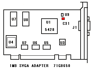 |
U1 CL-GD5428-80QC-A
U2 74F244D
U3 06H2194
U5 74F373D
U6 74F373D
U7 NEC-42S4260-70
or it's equivalents
U8 NEC-42S4260-70
U9 LM334
C31 Capaciotr ( soldered
reversed position.. by what reason) |
I thought this one was really a "BAD" MCA adapter IBM had ever
made. Probably the adapter worked *fine* when it was new.
But after several months ( or years ) of running in a system, it
became very flikery. All of 1MB SVGA /A in my hands give
me "Sandstorm" on my display. And actually IBM might
make mistake.
Peter Wendt found "wrong orientation" of a capacitor C31.
Click here
for the solution of "Sandstorm" disease. The page is an updated Louis's
1MB SVGA page mirrored by David L Beem. I'd like to quote Louis's
outline ( a little bit modified by me ) to compare Japanese CL-GD5428 SVGA
and Reply SVGA .
For electrical explanation, please read Peter's investigation and testing
reports by David L.Beem and Jim Shorney stored in above
mentioned page.
|
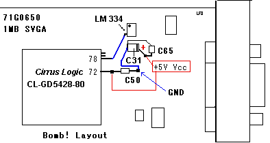
Note : Outlines of 71GG0650
were originaly created d by Louis Ohland
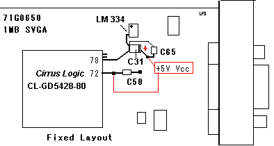 |
A) Remove the C31
capacitor and replace it to
newer one with same capacitance ( 2.2uF
16V
to 20V ) in REVERSE
orientation like Fig. left.
This rework is electrically equal to Reply
SVGA
layout.
B) Or remove the capacitor C31.
|
And, Untested
horrible thought.
2MB Hacking
Please reffer to this
page mirrored by David L. Beem. ( Seems nobody succeeded yet
)
@917B.ADF 5428
SVGA For Server500
-----------------------------------------------------------------------
AdapterId 0917bh
AdapterName "SVGA Adapter"
NumBytes 1
FixedResources
pos[0]=XXXXXXXXb
Begin Device 03h
NamedItem Prompt "ROM Address"
choice "C0000h-C7FFFh"
pos[0]=xxxxxxxxb mem 0C0000h - 0C7FFFh
Help
"This is the address range for the video adapter. This
address cannot be changed"
End
.
------------------------------------------------------------------------------
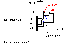
SOJ DRAM Pin Assignment
Peter Wendt wrote to the PS/2 News Group on 2002.03.01.
Chips listed below are commonly used for PC750, PC720 ( Japanese
Desktop PC ) and Reply PowerBoard.
For those that cannot locate a pinout on the 256K
x 16 DRAMs:
+--------------------------------------------------------------------+
|
|
|
Pin Assignment
|
|
256K x 16 DRAM
|
|
(40 Pin SOJ)
|
|
|
|--------------------------------------------------------------------+
| Fujitsu MB 814260
Goldstar GM 71C4260 |
| Hitachi HM 514260
Hyundai HY 514260 |
| Micron MT 4C16257
Mitsubishi M5M 44260 |
| Motorola MCM 54260
NEC UPD 424260
|
| OKI
MSM 514260
Samsung KM 416C256 |
| Texas Inst. TI 45160
Toshiba TC 514260 |
|--------------------------------------------------------------------+
|
|
|
|
|
/--------------+
|
|
Vcc --+o 1 40 +-- Vss
|
|
DQ1 --+ 2 39 +--
DQ16
|
|
DQ2 --+ 3 38 +--
DQ15
|
|
DQ3 --+ 4 37 +--
DQ14
|
|
DQ4 --+ 5 36 +--
DQ13
|
|
Vcc --+ 6 35 +--
Vss
|
|
DQ5 --+ 7 34 +--
DQ12
|
|
DQ6 --+ 8 33 +--
DQ11
|
|
DQ7 --+ 9 32 +--
DQ10
|
|
DQ8 --+ 10 31 +-- DQ9
|
|
nc --+ 11 30 +--
nc
|
|
nc --+ 12 29 +--
CASL#
|
|
WE# --+ 13 28 +-- CASH#
|
|
RAS# --+ 14 27 +-- OE#
|
|
nc --+ 15 26 +--
A8
|
|
A0 --+ 16 25 +--
A7
|
|
A1 --+ 17 24 +--
A6
|
|
A2 --+ 18 23 +--
A5
|
|
A3 --+ 19 22 +--
A4
|
|
Vcc --+ 20 21 +-- Vss
|
|
+--------------+
|
|
|
|
Vcc = +5V DC
|
|
Vss = 0V DC (GND)
|
|
|
|
Signal marked with # are active LOW !
|
|
|
|
|
| (Source: Micron Technology Inc. Datasheet
- ASCII Art by PHW) |
|
|
|
|
+--------------------------------------------------------------------+
PS/55 Index
|