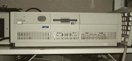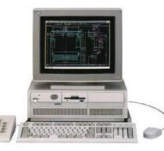
5560-W1B with "kit W2B"
Pictures for Processor complexes stored
in this page are originally created by
Louis Frederick Ohland.
You can see original pictures for PS/2 complexes
at Louis's
complex page.
General
information
5560-W, the first desktop model with 486 class CPU, was introduced
to the market on Oct. 1990 together with 5580-Y.
5560 uses same base/outer case with PS/2 Mod. 90, ( 8590
or 9590 ) but the planar and the processor
complexes are different from 8590 and 9590. Main differences are as
follows.
-
.
-
Two MCA BUS slots are prepared in stead of memory
riser connector.
-
SIMM sockets are directly mounted on the planar
-
XGA video is not ready on the planar.
-
Power connectors are not Edge Card type.
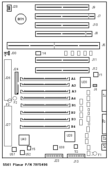
5560 Planar
All types of 5560 use same planar.
 |
J1 serial port
J2 Parallel port
J3 Mouse
J4 K/B
J5 Processor complex
J6 Power on pass word
J7 BVE 32-bit slot
J8 AVE 32-bit slot
J9/J10 32-bit slot
J11/12 32-bit slot
J13 Power
J23 Power
J24 FDD connector
J26 Solder pads
J27 Solder pads
J28 PWR/LED connector
J30 SP
Y1 40.00MHz
Y2 22.1148MHz
Y4 14.318MHz
Y5 24MHz
U20 57F2188
U28 64F0942
U43 N82077AA
U52 22V10-25 35F3798
U57 DSKBOOT 64F3110
F1 2A
F2 3A
F3 5A |
J11 & J12 are not for SIMM risers but they are
usual 32-bit MCA slots.
SCSI /A with cache is initially installed
at J12.
Japanese Display Adapter B-II ( or XGA-2
) is placed at J7.
Power connector
Edge card power connector is not used
on this planar. J13/J23 are pin type
connectors to which
female connectors from PSU are plugged.
Model-Types
As described in At
a glance page, there are 4 types of 5560.
5561-W0x ; 486DX25
You'll have enough time for cigarettes and a cup of coffee or two
until
the machine finish memory count if you have filled all SIMM socket
with
8MB SIMM.
5561-W1x ; 486SX25
Memory count is faster than -W0x.
5561-W2x ; 486DX2-50
Most likely the complex is same with -W1x.
5561-Nxx ; 486DX2-66
Supper charged 5560 with a Type-B DX2-66 upgrade platform.
5560-W
| Model |
5561
|
|
W08, W0B, W0C
|
W18, W1B, WYA, WYB
|
W28, W2B, WA8, WAB
|
| Processor |
486DX-25
|
486SX-25
|
486DX2-50
|
| RAM |
4MB
|
4MB ( 70ns)
|
4MB ( 8MB for WAx )
|
| VRAM |
1MB ( PS/55 Display Adapter ) B-2 ?
|
Disk
Drives |
FDD |
3.5" x1 ( 1.44MB/720KB )
|
| HDD |
Last digit of type code indicates HD capacity ( 8; 80MB, B; 160MB,
C; 360MB )
|
| Option Slots ( for users ) |
32bit full size x3 , 32bit half size x1
|
| Storage bay |
2
|
| Dimension ( mm ) |
440( W ) x 430 ( D ) x 140 ( H )
|
| Weight ( Kg ) |
14
|
| AC Input |
AC100--120V 50/60Hz, 215W ( MAX )
|
| OS installed |
None
|
WYx; S/2 J2.0 & DOS J5.0 |
WAx; S/2 J2.0 & DOS J5.0 |
5560-N
| Model |
5561
|
|
N0B
|
NYB *1
|
NMB *
|
NMY *
|
| Processor |
i486DX2-66
|
| RAM |
8MB
|
16MB ( 70ns)
|
| VRAM |
1MB ( PS/55 Display Adapter ) B-2 ?
|
Disk
Drives |
FDD |
3.5" x1 ( 2.88MB/1.44MB/720KB )
|
| HDD |
200MB
|
| Option Slot ( for User ) |
32bit full size x3 , 32bit half size x1 |
32bit full size x2, 32bit half size x1 |
| Storage bay ( for user ) |
2
|
| Dimension ( mm ) |
440( W ) x 430 ( D ) x 140 ( H )
|
| Weight ( Kg ) |
11.4
|
| AC Input |
AC100--125V 50/60Hz , 194W( MAX )
|
| OS installed |
None
|
OS/2 J2.0 & DOS J5.0 |
OS/2 J2.0 & MCADAM |
OS/2 J2.0 & MCADAM |
*1 NYB : OS/2 model
*2 NMB : MCADAM/2 ( CAD software ) included .
ASYNC TTL /Adapter is included.
*3 NMY : MCADAM/2 upgrade version.
ASYNC TTL/Adapter is included
SIMM
8 x 72pin SIMM sockets are directly mounted on the planar.
True parity 8MB/70ns SIMMs are mandatory for -W1, -W2 and -N
complex.
For W0 complex, 80ns SIMMs are standard and must be used in matched
pair.
For W0/W1 models, reference Ver. 1.11 is required to use
RAM's more than 16MB.
Video
No video chip is ready on the planar. PS/55 Display Adapter
B-2 ( BVE with VGA chip ) is used for 5560.
5560 doesn't have XGA chip on the planar.
AVE 32-bit slot locates beside complex riser in addition to BVE slot
which is already occupied with D/A B-2.
Genuine SCSI /A with
cache
A stock SCSI /A for -W1/W2 models is, unlike 8590, half
length 32 bit adapter with AT like 50 pin header .
ADF is usual @8eff ( 32Bit with cache ). SCSI micro code
set is 64F4376/4377. See outline HERE.
16 bit SCSI /A was used for W0 model but I don't know if it was
a long uncached card or short uncached card.
5560-N model was equipped with a short length SCSI Adapter II/A
(32bit) with 512KB cache ( which is IDed as 06G6760 in
sales leaflet and I think the part might be ether 35G2818
or 07G3063. )
Inner View
( click image to enlarge )
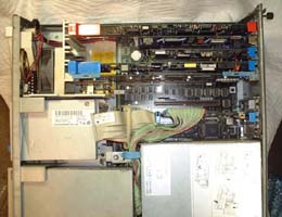
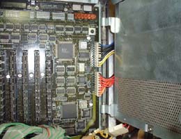
Photos below are inner view of my 5561-W1B with Type-B Upgrade processor
complex.
Half sized caching SCSI /32A with 50 pin header was changed to
a short caching SCSI /A -II/32A with new micro code set.
You can see an AM5x86-133 on an interposer with
a short height heat sink which runs in 160MHz inner
speed ( No CPU fan but fresh air blows out from the front fan
).
Pic #1 ( click pic to get JPEG,
63KB )
 |
Adapters ( from top )
J9 ; Madge Smart Ringnode MC32
J7 ; XGA2
J10 ; ACPA
J8 ; Intel Fax/Modem Adapter
J5 : Processor complex DX2/66 Up Grade
Type-B
J11 ; vacant
J12 ; Short Cached SCSI with new Microcode
 Close view of CPU #1
 Close view of CPU #2
|
|
|
Pic #2 ( click pic to get JPEG,
84KB )
 |
Close View ; SIMM and Power Connectors
You can pull the PSU upward and then swing it down to
right side like Mod. 95.
You can see Power connection is different from
PS/2 Mod.90.
Tall height SIMMs are not good for 5560.
Needs clearance between SIMM and the PUS. |
|
|
Processor complex for 5560
( please see comparing
chart )
Following complexes can only be used with 5560 planar except
W0 complex which can be used for 5580 if you want.
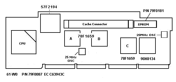
W0 ;
P/N 79F0087, 80486DX-25MHz.
Seemed to be a Modified Type 1- J. 256K cache card available.
No overdrive socket prepared.
This complex can take 31 MHz OSC without any change of BIOS.
The Board design is same with 5580-Y complex. BIOS P/N are same each other
but just the board P/N and FUR and OSC are different ( 5580-Y0 uses
33.3MHz OSC ). |

* Original image
was outlined by Louis F. Ohland
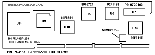
W1 ; P/N 07G0460
FUR 95F4299, 80486SX-25MHz.
Modified Type H.
486SX CPU is loaded on the main socket ( U8 ) and an overdrive socket is
placed right
next to the main socket. Memory count is faster than
W0 complex.
No L2 cache available.

* Original image was outlined
by Louis F. Ohland *
W2 ; P/N 07G3153 
( amended on 2003.05.04)
My machine is labeled as "5561-W1B"
and has a sticker "KIT-W2B".
KIT-W2B description.
A sticker "P/N 07G3153"
and REA number is attached right on the area ( the solder side of
U8,
80486DX socket) where P/N is silk
screened on a W1 complex.
Also there is a " MPU Upgrade"
sticker attached on the blue lock lever of the complex board.
Earlier W2x models were shipped
with an i486SX-25 loaded on socket U8 and a 486-25/50 upgrade
option ( ID#06G7015 ) on
socket U9. Latter models were shipped with i486DX2-50 loaded
alone on
the socket U9. W1
and W2 complexes are "same" each other.
U6
Variants from Louis's page
" Some Type-2 (92F0079)
suffer from an "incompetent DMA-chip", which is P/N 92F1428 at
position U6/GA-M on the card. Working Type-2s 92F0079 have a DMA-chip P/N
10G7808
at U6/GA-M. If U6/GA-M is 10G7808 a Turbochip should work fine.
The earlier Type-2 use the 92F1428 - which ends the experiment in
odd results (permanent
I9990044, 605 FDD errors, permanent 165 errors and inability to read from
FDD). "
But Japanese
" KIT-W2B" with U6 P/N 92F1428 works fine with ;
1). DX4ODP-75
with 486SX25 on the 1st socket.
2). DX2-66
alone on the 2nd socket ( 50MHz inner clock operation )
3). DX4-100
on an interposer with VRM alone on the 2nd socket.
4). am5x86
or Cyrix 5x86 ( with voltage interposer )on the 2nd socket.
There is no significant difference
between Type 2 H in Louis's page and above PS/55-W1/W2
complex. The board P/N (
or FRU ? ) and the BIOS P/N are just different.
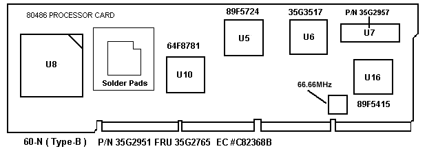
N ; P/N
35G2951 FRU 35G2765 80486DX2-66MHz 
A variant of
Type 2- L?
No support for SyncroStreaming
Data transfer.
Originally equipped
in Model 556-N which was introduced to the market in Sep.1992.
The complex is also
referred as DX2-66 UpgradeType-B .

* Original GIF
image was outlined by Louis F. Ohland *
There is no over drive
socket on this complex. At the position of U9 of W1/2
complex,
N complex has solder
pads.
DMA controller chip
U6 is 34G3517 for N and
92F1428
for W1/2.
At least there are
2 versions of this complex. While I replaced the OSC to
80MHz, I noticed
that copper traces
around solder side of OSC were different, and found one board has a chip
resister and the other
doesn't. Both complexes worked fine with 80MHz OSC with
modified
BIOS ROM.
All complexes of model
5560 including N complex use EPROM.
Streaming data transfer
feature is not supported on all 5561 complexes.
CPU upgrade:
For Wxx, DX4ODP-75 can be used. You can use DX4ODP-100
but it runs in 75MHz inner speed.
N model can take DX4-100, AMD and Cyrix
with an appropriate VRM interposer which supplies
3.3v - 3.45v. As N complex has it's CPU socket at
the front edge, it's difficult to use a thick heat
sink with a cooling fan in regular size. As far
as you use blue plastic air guide properly, your CPU
will get fresh air flow from the front fan.
Complex upgrade:
60-W0/W1 can be replaced to -W2 or -N complex,
60-W2 can be replaced to -N complex.
60-W1/W2 complexes can be used for 5580. Associated
REF/DIAG for 5560 could not be used
in this case. REF/DIAG for 5580-Wxx should be used
together with.
5580 with 60-W0 complex with 5580-Y REF/DIAG
==> No equivalent model exist but works fine.
5580 with 60-W1 complex with 5580 -W REF/DIAG ==>
5580-W0x
5580 with 60-W2 complex with 5580-W REF/DIAG ==>
5580-W2x
My 5561-W1x ( upgraded with 60-N complex )
64MB of RAM, BIOS modified N complex with
80MHz OSC, am5x86 running x4 speed,
ATI-GUP, Madge Ringnode MC32, Genuine
IBM SCSI /32A with cache, 650MB+1G hard drive,
Hitachi made x2 CD-ROM without bezel.
F/W SCSI-2 /A in 5561
PS/55 Index
|
