|
General information
Japanese variants of PS/2 8570.
5550-S/T, the first Desk Top model of PS/55 line, were introduced
to the market in Apr.1988 together with 5570-T ( 8580-20MHz analogous ).
5550-S/T were basically same with PS/2 8570. IBM Japan
modified 8570 in some way. A most distinctive difference was the number
of MCA slots. 50-S/T has four MCA slots.
The 4th slot was added for Japanese Display Adapter to handle Japanese
characters on PS/2.
Thus 5550 planar was wider than that of PS/2 and, as a matter
of fact, the body was also wider than 8570.
Except the width, 5550 and 8570 were almost same cosmetically.
The planar of earlier models of S and T had some problem regarding
BUS Mastering feature and those planars were called Stage-1 and the models
with free from this problem were called Stage-2. So there should
be 4 types of planars for S and T models and another one ( or two
) for 25MHz version.
Easy way to identify stage-1 and stage-2 .
If the Power SW lever is RED, most possibly
it's Stage-1.
If the Power SW lever is WHITE, maybe
it's Stage-2.
Identifying with serial numbers.
Even if the Power SW is white, systems with
following serial numbers belongs to Stage-I
5551-S09 S/N before 97-19300
5551-T09 S/N before 97-44700
5551-T0A S/N before 97-58000
5551-T0B S/N before 97-93100
Brief Chart of 5550 and Industrial 5500 models based on PS/55
System Guide
O: means the model is listed in the Guide Book
+ UG: means 486DX upgrade option is also listed
|
5550-S |
5550-T |
5550-V0 |
5550-V1 |
5550-V2 |
|
5502-S/T |
5502-TG |
5502-V2 |
5502-VG |
| 1988-07 |
O
|
O
|
|
|
|
|
|
|
|
|
| 1988-12 |
O
|
O
|
|
|
|
|
|
|
|
|
| 1989-06 |
O
|
O
|
O
|
|
|
|
|
|
|
|
| 1990-02 |
O
|
O
|
O + UG
|
|
|
|
O
|
|
|
|
| 1990-07 |
S1 O
|
T1 O
|
|
O + UG
|
|
|
O
|
|
|
|
| 1990-11 |
S1 O
|
T1 O
|
|
O + UG
|
|
|
O S1/T1
|
O
|
O
|
|
| 1991-05 |
S1 O
|
T1 O
|
|
|
O
|
|
O S1/T1
|
O
|
|
O
|
| 1992-02 |
|
|
|
|
O
|
|
O S1/T1
|
O
|
|
O + UG
|
Most possibly switch over to Stage-II from Stage-I was made around May
to Jul in 1990.
As for 5530, 5530-T04/T08 ( Stage -II ) and 5530-S12/S14
( ZSX on Stage -II ) were listed in 1990 Nov. edition.
Reference
Ref. Ver. 1.00 to Ver.1.36 are based on JDOS.
Ref. Ver higher than 1.4x are based on DOS/V.
Ver. 1.50 covers most of of all 386 models such as 5550-S/T/V,
5570-T/V, 5540-T, 5530-T.
Video
For S, T and Vo/V1 models
As like as PS/2 8570, PS/55 5550-S/T have VGA
chip on the planar. But in order to handle true Japanese fonts,
PS/55 Japanese Display Adapter II ( with AVEC
connector ) is equipped with earlier models of 5550-S/T ( and 5570-T ).
VGA port on the planar is covered with a plastic plug.
For V2 model.
I'm not sure about a display adapter used for this model.
V2 planar does not have a VGA chip and it has BVE MCA slot. Then most
possibly Display Adapter B or B-2 might be equipped with V2 model.
Memory
P/N
capacity Remarks
65X1211 2MB
5550-S/T
65X1212 4MB
5550-T. Double-decked shape. Only one module can be used.
This module should be installed at J9( memory slot #3)
23F2165 4MB
5550-V0/V1. Double-decked ?
79F2536 4MB
5550-V, 5541-T, 5530-S/T, 5510-T
79F2500 8MB
5550-V, 5541-T, 5510-T
Hard Disk
interface
Same as 8570, ESDI ( roughly speaking ).
Planar
There were various types of planar for 386-class 5550
| Model |
CPU |
Planar Level |
MCA Slots |
| S |
16MHz |
Stage-1 & Stage-2 |
4 Slots |
| T |
20MHz |
Stage-1 & Stage-2 |
4 Slots |
| V0/V1 |
25MHz |
|
not sure, most possibly 4 |
| V2 |
25MHz |
|
5 slots, No VGA chip on the planar |
I've once heard that S stands for
Sixteen,
T stands for Twenty and V stands for twenty
fiVe.
Back to Top
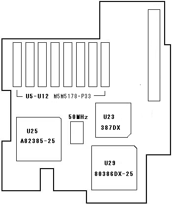
Stage- 1
Planar ( 16MH/20MHz)
Following outline is a stage-1 T planar. Don't know how it differs
from Stage-1 S planar. But most possibly these might be same except OSC
Y5.
Following stage-1 20MHz planar looks like 8570
type 1 planar |
20MHz T Planar P/N 65X1377, EC 341537S
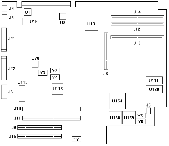
J3 Mouse Connector
J4 Key Board Connector
J5 Speaker
J6 VGA
J8 FDD/HDD Riser Connector
J9 16 bit MCA Slot ( AVE
)
J10 32 bit MCA Slot
J11 32 bit MCA Slot
J12 MEM.LOCATION 3
J13 MEM.LOCATION 1
J14 MEM.LOCATION 2
J15 16 bit MCA Slot ( AVE )
J21 Parelel
J22 Serial |
U1
LM340
U8 72065L
/ NEC D72065L
U13 PIO / 72X8299
U16 8042 / 72X8455
( BIOS ? )
U70 NS16550 / NS16550AV
U111 27512 / 23F3012
U113 IMSG170 / IMSG171P-35
U115 VGA / 90X8941
U128 27512 / 23F3013
U154 80386 / i80386DX
U159 80387 co-pro socket
U168 DMA / 90X8134 |
Y2 25.175MHz
Y3 1.8432MHz
Y4 28.322MHz
Y5 40.0000
Y6 32.0000
Y7 14.318MHz |
Stage-2 Planar
( 16MHz/20MHz )
Recently I had a chance to see stage-2 20MHz planar and noticed it
is totally same with my Stage-2 16MHz planar except installed OSC Y1 and
planar P/N.
-
Aside from the
fact that 5550 has 4 MCA SLOT, Layout
of Stage-2 planar is different from that of 8570 in following
points.
-
5550 Stage-2 planar has only one SIMM socket on the planar. another
2 sockets are placed on the Expansion card which is connected to the planar
through J3.
-
BUS riser J7 is moved left ( moved downward in the outline below ),
hence HDD/FDD riser is different from stage-1 model and that of 8570
type-1 )
-
Speaker/Battery connector is not a riser type. SP/BT ASM is connected through
wire and a male plug like 8580.
-
ZIP VRAMs are directly mounted on the planar.
See below and compare the planar with 8570
Type-1 outlined by by Louis.
Stage-II planar;
P/N 38F6776 for S( 16MHz ) and 54G1612 for T ( 20MHz )
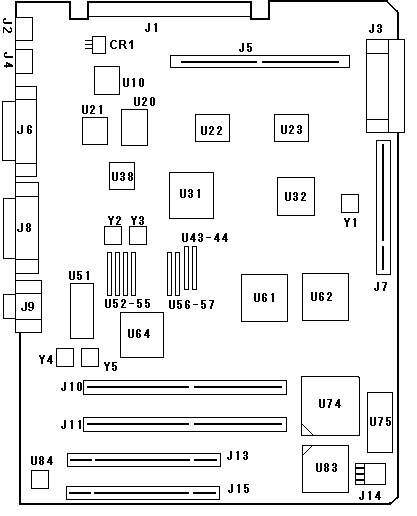 |
J1 Power
connector edge card
J2 Keyboard
J3 Mem
expansion connector
J4
Mouse
J6 Parallel
J7
Bus Riser
J8 DB25
serial
J9 HD15
Video
J10,11 32-bit
slot
J13 16-bit
AVE slot
J14 Speaker/Battery
connector
J15 16-bit
AVE slot
U10 NEC
72065L
U20 33F8602/FDC
U21 NS16550AFV/UATR
U22 33F5946/CPUGA
U23 33F5944/MEMCTRLGA
U31 33F5938/IOCTRLGA
U32 38F6972/EPP3GA
U38 N8042A/90X9298
U51 LM339
U52-57 M5M446AM--12(VRAM)
U43-44 ditto
U61 57X4211
U62 90X8134
U64 90X8941/VGA
U74 80386DX-16
U75 BIOS
U83 co-pro
socket
U84 MC146818
Y1
32MHz for S, 40MHz for T |
SYSTEM MEMORY
EXPANSION CARD for 5550-S/T stage -2 planar
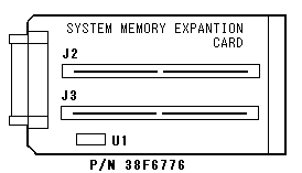 |
J1
102P connector to Planar J3
J2 MEM location 3
( 2MB/4MB memory slot )
J3 MEM location 2
( 2MB memory slot )
U1 LS244 ( SN74LS244N
) |
Back to Top
Back to Top
V0/V1 ( 25MHz
) Planar
--- Not Available Now -----
V2 (25MHz)
planar
As a matter of fact, I have not actually examined complete
V systems ever. I just have a V2 planar. When I
draw outline of the planar, I noticed that 25MHz V2 planar doesn't
have onboard VGA. Man, this planar has 5 MCA
slots
and, to my surprise, there are solder pads for another 16-bit
slots!
BUS riser slot J6 is shifted to the left comparing S planar I have.
It means there should be more than three types of
BUS Riser Card. Locations of BUS riser connectors are
different with each other. |
25MHz V2 planar
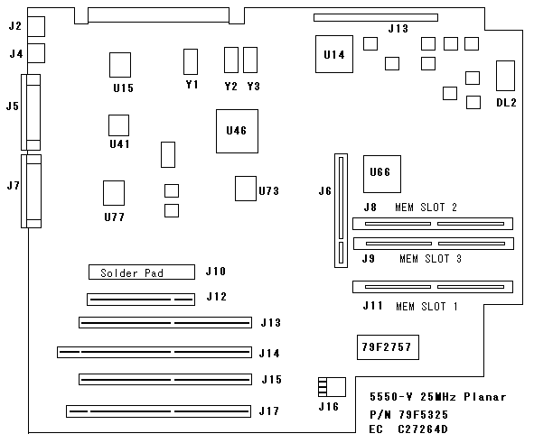
J1
Power connector edge card
J2 Mouse
J3 Connector
( CPU sub-board )
J4 Keyboard
J5 Parallel
J6 Bus riser
( watch the location )
J7 DB25 serial
J8 Memory slot
#2
J9 Memory slot
#3
J11 Memory slot #1
J10 Solder pads for 16-bit
slot
J12 16-bit slot
J13 32-bit slot
J14 BVE 32-bit slot
J15 32-bit slot
J17 AVE 32-bit slot
J16 Speaker connector |
DL2 TQW-100
U14 90X8134
U15 N8042( 90X9298)
U41 56F7502/ISERE
U46 72X8299/PIO
U66 57X4311
U73 NEC D72560L
U77 NS 16550
BIOS P/N 79F5325
Y1 32.0MHz
Y2 14.3MHz
Y3 40.0 MHz
Y4 1.8432MHz |
CPU Daughter
Board
Main
differences between 8570 sub board and 5550-V2 sub-board are
1)
Pin orientation of 387 co-pro
2)
Planar-daughter board connector.
Memory
From 5550-V2 system guide;
One 4MB
SIMM was originally installed, expandable up to 16MB on the planar.
Option
SIMM's are
1) 4MB P/N 79F2536
2) 8MB P/N 79F2500 ( only one module can be used
on a planar )
Clock Rodding
A guy once reported
that he had changed 50MHz OSC to 60MHz and system worked without
POST error.
Back to Top
Riser
card for HD and FDD
As written in V planar section, there are several types
of BUS riser cards. I once had two types of riser card but
there should be three or more.
CPU upgrade
I tested following upgrade kits on my S and T models.
1. Evergreen upgrade modules with IBM486BL2 and BL3.
Cyrix and TI chips could be used on S/T models
but not on V models due to 64K L2 cache on the
CPU board ( I have not examined. ).
2. Kingston MC master 486 ( originally made by AOX ).
I used it on T planar. MCMaster can
take a 5x85 CPU but you can't use neighboring MCA slot in
order to use 5x86 CPU with a heatsink. Not
a good choice for 8570 because it has only 3 MCA slots.
3. PowerBoard
In order to use a PowerBoard on S( Stage-II
) model, some adjustment is needed to place the board
properly.
1) Need to adjust location of
metal parts for screw holes to keep the planar.
Location of
screw holes at left front edge is different between S and T/V.
2) a BUS Riser card for FDD and ESDI
hard disk for T model.
3) battery and SP unit for T model.
Genuine option by IBM
80486-25Mhz Processor Upgrade Kit ( P/N 57F0085 ) was listed
for 5551-V0x model.
5502
5502 is an industrial model number.
Industrial models are numbered as " 5500" and each model has unique
number such as 5502-S1x, -T1x and so on.
| Type |
CPU |
Memory
|
HD
|
FDD
|
Option Slot
|
|
STD
|
MAX |
32/16bit
|
16bit
|
| S01 |
16MHz |
2MB
|
16MB |
-------- |
1
|
2
|
1
|
| S11 |
16MHz |
2MB
|
16MB
|
---------- |
1
|
2
|
1
|
| T19 |
20MHz |
2MB
|
16MB |
30MB |
1
|
2
|
1
|
| T1A |
20MHz |
2MB
|
16MB |
60MB |
1
|
2
|
1
|
| T1B |
20MHz |
2MB
|
16MB |
120MB |
1
|
2
|
1
|
| TFx |
20MHz |
2MB
|
16MB
|
|
1
|
Poss same with TGx |
| TGA |
20MHz |
2MB
|
16MB |
60MB |
1
|
4 *
|
1
|
| TGB |
20MHz |
2MB
|
16MB |
120MB |
1
|
4 *
|
1
|
| V2A |
25MHz |
4MB
|
16MB |
80MB |
1
|
3
|
2 ( half )
|
| V2B |
25MHz |
4MB
|
16MB |
160MB |
1
|
3
|
2 ( half ) |
| VGA |
25MHz |
4MB
|
16MB |
80MB |
1
|
3
|
2
|
| VGB |
25MHz |
4MB
|
16MB |
160MB |
1
|
3
|
2
|
Number of Option Slot
System Guide describes number of Option Slots left for users except
already occupied with a Display Adapter.
So basically, one slot should be added to the number shown in a diagram.
Model S11 to T1B meet with the rule and one 16bit AVE slot might already
be occupied with a display adapter. Then how it comes that TGA and
TGB were noted as 4 + 1 ? Wonder if these 2 models were
not shipped with any Display adapters and use VGA on the planar?
Next question; it seems models Vxx models DO have
activated 16bit 6th slot shown in outline of 5550-V2 planar. 5550-V2 planar
has four 32/16bit slots including x1 AVE and x1 BVE slot. But above diagram
shows 5500-V have three 32/16bit slots and two 16bit slots.
If 32/16bit BVE slot was occupied with a Display adapter, total MCA slots
would be SIX including two of 16bit slot. Would like to see
the planar. |
Back to Top
PS/55 Index Page
|
