Serial Port to
75150 / 75154 Pinout
Serial
Port Controller (HITR chapter, PDF)75150 Dual Line Driver Datasheet RS232C, SE Output, 2 drivers
75154 Quadruple Line Receiver Datasheet RS232C, SE Output, 4 drivers
1985 TI Linear and Interface Circuits Applications Vol 2
Section 9 Data Transmission pg 66-135
7515x stuff is pretty much pages 87- 95... "ish" YMMV...
PS/2 serial port, 75150 and 75154 relationship [thread on VCF, erudite comments]
Eudimorphodon and gslick helped me to wade through the absolute ABSENCE of ANY documentation from IBM. After more finger Ninjitsu and deep meditation, I will extract the good information in their posts.
NOTE: This was very messy, at the start I had nothing but datasheets and component IDs. The two co-conspirators had to delve deeply into past serial port construction so as to help "fit" the function of the 7515x combo.
PBC9FV2 DB9 Female Breadboard Adapter from Winford
NOTE: To me, the pin header points down, and that prevents me from easily seeing the pin number. Winford will modify an existing model for a minimum of 20+ units... BUT, they sell the individual components.
My desire...
Here are the individual components for the PBC9FV2 and PBC25F.
Item Description
--------------- ------------------------------
Z_PBC9FV2-PCB PBC9FV2 PCB
CNR9F-XF-CF-RC DB9 Female R/A PCB Connector
SH10P Single Row 0.1" Pin Header, St
Z_PBC25F-PCB PBC25F PCB
CNR25F-XF-CF-RC DB25 Female R/A PCB Connector
SH26P Single Row 0.1" Pin Header, St
NOTE: IBM sold you Technical References, which had enough for you to develop compatible devices and applications. One might accuse IBM of keeping the good stuff for itself, but think of the self-inflicted carnage caused by using a MOSTLY tame feature in a highly critical production system, and the "performance tweak" causes the system [network, server, process] to halt. HARD. Think of the COST of that service call to IBM. Cheaper to just not include that little factoid...
Serial Port and 75150 / 75154 Combination
Lorenzo Mollicone was demonstrating the differences between the 335w and 400w PSU in a 95XP. Taking one for the team, he smoked U29, but good. But, as I started to do a remote dissection, it didn't make sense that U29 had been turned into Swiss Cheese.
95XP Blown SN75150 IC
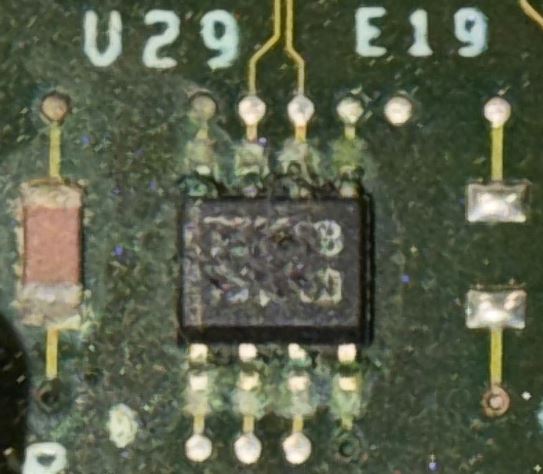
The 75150 surface is not blown out, but it looks "bubbled".
95XP 7515x Combination
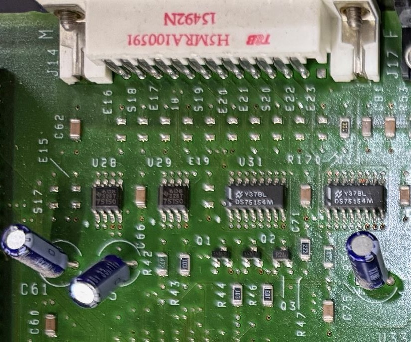
Here we have the single DB25 serial port on a 95XP. On the left, we have a pair of 75150 [U28, U29]. On the right, we have a pair of 75154 [U31, U34]. You will see a similar set-up on all IBM manufactured Micro Channel PS/2 systems. At present, Lorenzo is helping me determine the pinout of the 7515x / serial port pinout.
Bermuda 7515x Combination
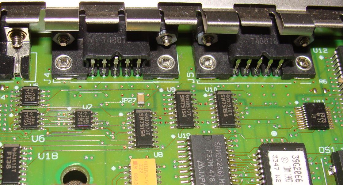
This illustrates the 7515x combination for two DE9 serial ports. Three 75150 are on the left [U5-7] and three 75154 are on the right [U8-10].
DE9 Pinout
[Bermuda]
|
Pin |
Signal |
|
1 |
Data Carrier Detect |
|
2 |
Receive Data |
|
3 |
Transmit Data |
|
4 |
Data Terminal Ready |
|
5 |
Signal Ground |
|
6 |
Data Set Ready |
|
7 |
Request To Send |
|
8 |
Clear To Send |
|
9 |
Ring Indicator |
8580 Serial Port Schematics [non-IBM, page 7]
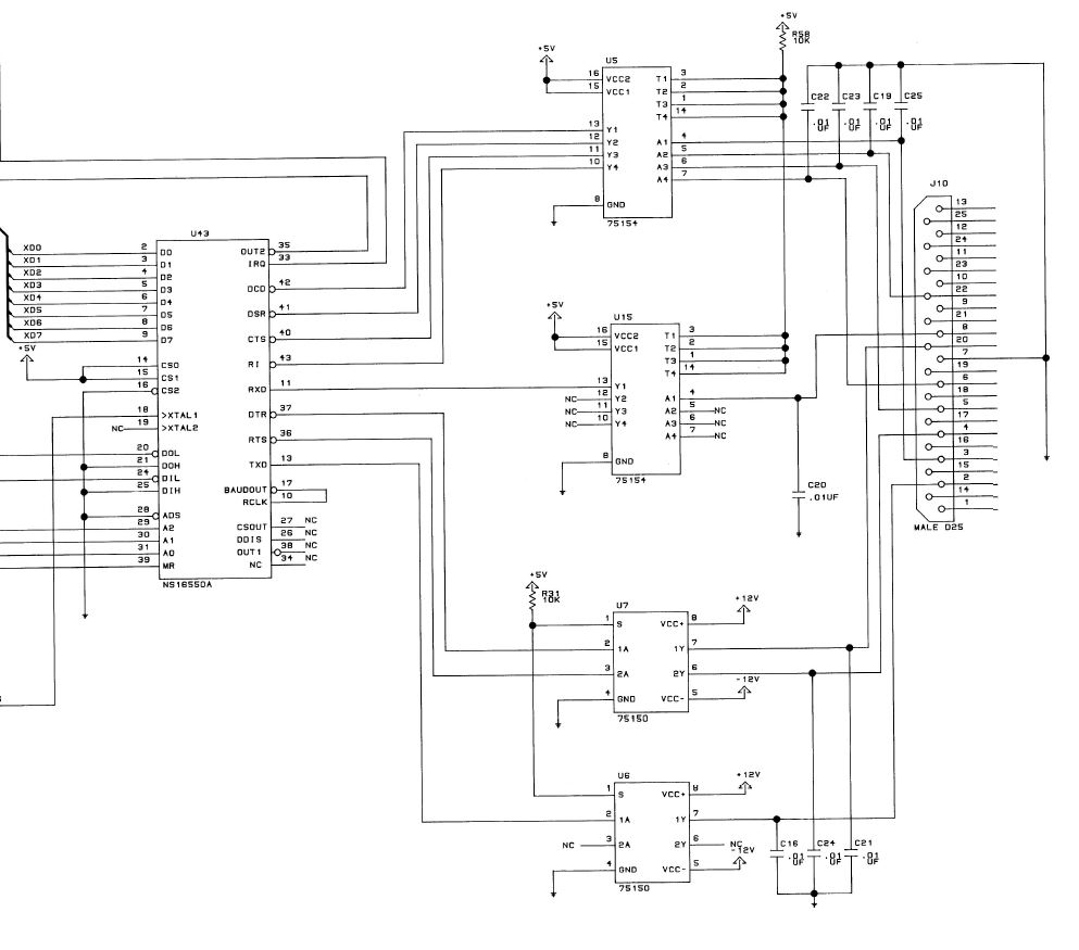
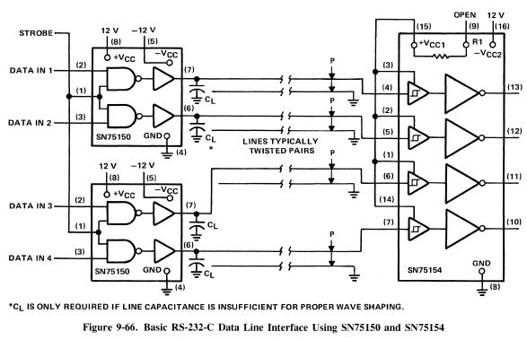
Folks, this 75150 / 75154 combo really has blown my mind. It is a level translator, interfacing the TTL logic [0v to +5v] of the UART / ASIC on the planar/sysboard to the RS-232 Bipolar [-12v to +12v] of the DB25 or DE9 connector.
If IBM could have integrated the signal level translator into the ASICs, it would have. They wouldn't have to run traces for the 7515x ICs, nor would they have to actually install the three to six 7515x ICs.
There are two possible reasons for the external level translators. First, they could be sacrificial, the smaller, cheaper and easier to rework ICs would burn BEFORE the big ASIC. Second, maybe the ASIC gates cannot handle a short circuit of the serial outputs.
Model 80 (8580) Serial Port Schematics look at page 7
It shows that all signals to and from the UART go through the 7515x combo. Ooohhh... The pinout on the schematics does not seem to fully match the HITR
Serial Port Controller (48 pages)
The Type 1 and Type 3 both use the 7515x combo.
The T1 uses a 1.8432 MHz osc with a divisor from 6-2034
The T3 uses a 22.1184 MHz osc [/2] to furnish an 11.0592 clock, divisor of 2-13824
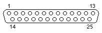
DB25 to 7515n Pinout
WIP...
DB25 Serial Port Pinout from Tech Ref
95XP DB25 Serial Port Populated Pins Image from Lorenzo Mollicone
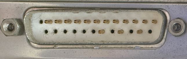
|
Pin |
Signal |
Pin |
Signal |
|
1 |
N/C [No Pin] |
14 |
N/C [No Pin] |
|
2 |
Transmit Data |
15 |
N/C [No Pin] |
|
3 |
Receive Data |
16 |
N/C [No Pin] |
|
4 |
Request To Send |
17 |
N/C [No Pin] |
|
5 |
Clear To Send |
18 |
N/C [No Pin] |
|
6 |
Data Set Ready |
19 |
N/C [No Pin] |
|
7 |
Signal Ground |
20 |
Data Terminal Ready |
|
8 |
Data Carrier Detect |
21 |
N/C [No Pin] |
|
9 |
N/C [Pin] |
22 |
Ring Indicator |
|
10 |
N/C [Pin] |
23 |
N/C [No Pin] |
|
11 |
N/C [Pin] |
24 |
N/C [Pin] |
|
12 |
Reserved [Pin] |
25 |
N/C [No Pin] |
|
13 |
N/C [Pin] |
|
|
NOTE: I have read-up on early variants of serial ports that used DB25 ports. Some had two complete serial ports and a 25-pin connector fully populated. IBM used the DB25 up to the 95XP and the Model 90. But a DE9 was used along with a DB25 on the Model 90.
There is a [slight] chance that IBM used pin 12 [Reserved] in conjunction with the ROLMphone, sort of a neat-o hybrid voice -AND- 56k "modem" over the 9051 [?] PBX. Though a most intriguing facet of the Holy Micro Channel, the ROLMphone doesn't do much without the PBX :(
Electrical Characteristics of RS-232
The standard defines the electrical specifications for the transmitting and receiving circuitry. To begin with, transmitters must be allowed to withstand indefinite short circuits either to each other or to the signal ground with no permanent damage. Receivers must meet the following input impedance requirements: their resistive load shall be between 3K and 7K ohms and their capacitive load shall not exceed 2500 picofarads [should be on a 50ft cable]. Also spelled out are the maximum and minimum rise and fall times for all RS-232 signals. Beyond this, things get a little confusing.
RS-232 Input and Output Levels
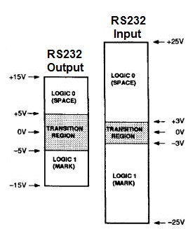
For instance, all the voltage levels involved do not correspond to conventional TTL logic levels for 1 's and 0's. RS-232 outputs are defined as follows: +5V to +15V is a logic "0" (Space); -5V to -15V is a logic "1" (Mark); and +5V to -5V is the transition region.
RS-232 inputs are defined in a similar fashion but with a narrower transition
region and able to tolerate wider voltage swings: +3V to +25V is a logic "0"; -3V to -25V is a logic "1 "; and +3V to -3V is the transition region. As you can see, RS-232 is still a binary logic system with only 2 allowable voltage ranges. The transition region (approximately "0" volts) is not allowed and having either an output or an input in this condition would indicate a problem.
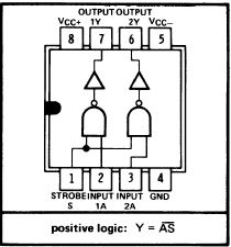
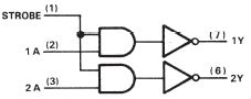
75150 Pinout
 |
 |
| Pin |
Function |
Pin |
Function |
| S 1A 2A GND |
Strobe Data Input 1 Data Input 2 Device Ground |
Vcc+ 1Y 2Y Vcc- |
+12Vdc Inverted Output 1 Inverted Output 2 -12Vdc |
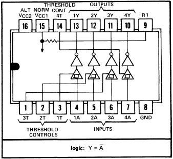
75154 Pinout
 |
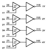 |
| Pin |
Function |
Pin |
Function |
| 3T 2T 1T 1A 2A 3A 4A GND |
Threshold 3 Threshold 2 Threshold 1 Input 1 Input 2 Input 3 Input 4 Device Ground |
Vcc2 Vcc1 4T 1Y 2Y 3Y 4Y R1 |
+12Vdc +5Vdc Threshold 4 Inverted Output 1 Inverted Output 2 Inverted Output 3 Inverted Output 4 Resistor |
The SN75154 is a monolithic quadruple line receiver designed to satisfy the requirements of the standard interface between data terminal equipment and data communication equipment as defined by EIA Standard RS-232C. Other applications are for relatively short, single-line, point-to-point data transmission and for level translators. Operation is normally from a single five-volt supply; however, a built-in option allows operation from a 12-volt supply without the use of additional components. The output is compatible with most TTL and DTL circuits when either supply voltage is used.
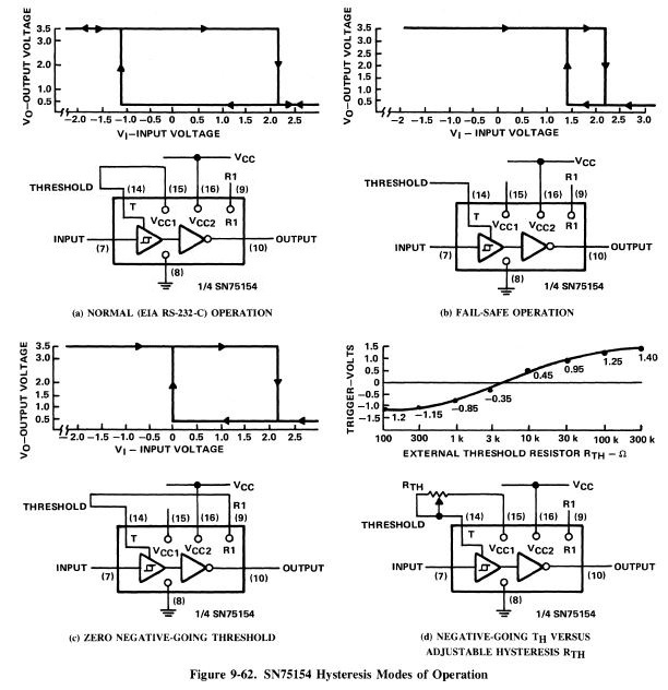
In normal operation, the threshold-control terminals are connected to the Vcc1 terminal, pin 15, even if power is being supplied via the alternate Vcc2 terminal, pin 16. This provides a wide hysteresis loop which is the difference between the positive-going and negative-going threshold voltages. See typical characteristics. In this mode of operation, if the input voltage goes to zero, the output voltage will remain at the low or high level as determined by the previous input.
For fail-safe operation, the threshold-control terminals are open. This reduces the hysteresis loop by causing the negative-going threshold voltage to be above zero. The positive-going threshold voltage remains above zero as it is unaffected by the disposition of the threshold terminals. In the fail-safe mode, if the input voltage goes to zero or an open-circuit condition, the output will go to the high level regardless of the previous input condition.
75154 Hysteresis Modes of Operation
Basic RS-232-C Data Line Interface Using SN75150 and SN75154