| Proc. Name |
Specified processor | MHz | Socket type |
pins | PGA | Volt I/O |
Volt core |
|---|---|---|---|---|---|---|---|
| P4 | i80486DX | ||||||
| P4S P23 |
i80486SX | ||||||
| P23S P23N |
i80487SX | ||||||
| P23T P4T |
i80486 Overdrive for 80486 (169 / 168 PGA) |
||||||
| P24 P24S |
i80486DX2 | ||||||
| P24D | i80486DX2WB | ||||||
| P24C | i80486DX4 | ||||||
| P24CT | i80486DX4WB | ||||||
| Proc. Name |
Specified processor | MHz | Socket type |
pins | PGA | Volt I/O |
Volt core |
| P5 | Pentium® | 60 or 66 | 4 | 273 | 21x21 | 5V | 5V |
| P24T | Pentium® Overdrive for 80486 |
63 or 83 | 3 | 237 | 19x19 | 5V | 3.3V |
| P54C | Pentium® | 75+ | 5 7 |
320 321 |
37x37 | 3.3V | 3.3V |
| P55C | Pentium® with MMX | 166+ | 7 | 321 | 37x37 | 3.3V | 2.8V |
| P54CTB | Pentium® with MMX Overdrive for Pentium® |
125+ | 5 7 |
320 321 |
37x37 | 3.3V | 2.8V |
| P6 | Pentium® Pro | 8 | 387 |
PGA - Pin Grid Array
Socket Type-7 may utilize a VRM (Voltage Regulation Module). A VRM allows
different CPU Voltages to be supported by interchangeable VRM's. A VRM would be
common for very high CPU MHz rates and / or when a precise core voltage is needed.
(On the PC-700 Series, the VRM socket is a 30-pin two row header.)
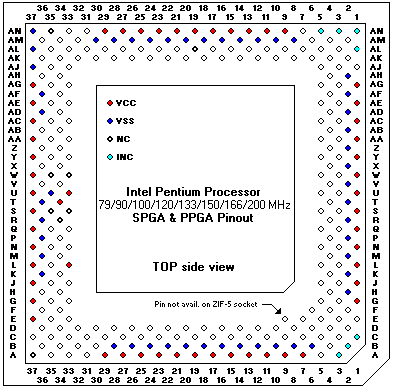
Pentium® ZIF-5 & ZIF-7 Socket. (320/321-pin)
Pentium® Processor Block Diagram
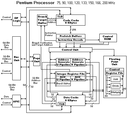
The (above) block diagram shows the two instruction pipelines, the U pipe and the V pipe. The U-pipe can execute all integer and floating point instructions. The V-pipe can execute simple integer instructions and the FXCH floating-point instructions.
The separate code and data caches are shown. The data cache has two ports, one for each of the two pipes (the tags are triple ported to allow simultaneous inquiry cycles). The data cache has a dedicated Translation Lookaside Buffer (TLB) to translate linear addresses to the physical addresses used by the data cache.
The code cache, branch target buffer and prefetch buffers are responsible for getting raw instructions into the execution units of the Pentium® processor. Instructions are fetched from the code cache or from the external bus. Branch addresses are remembered by the branch target buffer. The code cache TLB translates linear addresses to physical addresses used by the code cache.
Back to
Please see the LEGAL - Trademark notice.
Feel free - send a  for any BUG on this page found - Thank you.