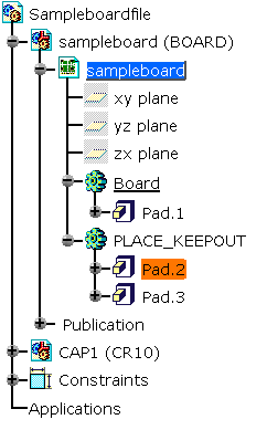
The place keep-out area (Pad.2) is displayed in transparency.
 |
-
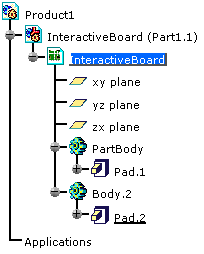
Right-click the Pad.2 in the specification tree to display the contextual menu.
-
Select Properties.
The Properties dialog box opens. -
Click More... .
The Circuit Board Design tab appears. 
-
Select Circuit Board Design.
-
Enter 6mm in the Maximal height field and 2mm in the Minimal height field.
-
Then click OK.
The pad is updated: the maximal and minimal heights are linked to the pad limits.
It represents the overall dimensions of the constraint area.
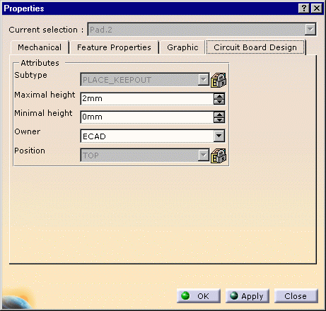
This attribute is recognized and displayed in the Circuit Board Design tab.
This attribute is managed only on the idf file import.
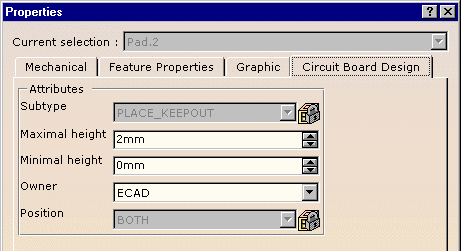 |
They share the same properties: modifying the properties on one pad will modify them on the other pad.
 |