Because efficient use of caches is a major factor in achieving high processor performance, software developers should understand what constitutes appropriate and inappropriate coding technique from the standpoint of cache use. Achieving that understanding requires some knowledge of the RS/6000 cache architectures.
The following discussion is for the benefit of programmers who are interested in the effect of caches and virtual addressing on the performance of their programs. Engineers who are interested in the details of the electronic logic and packaging of the RS/6000 will find it oversimplified, and the distinctions among the POWER, PowerPC, and POWER2 architectures blurred.
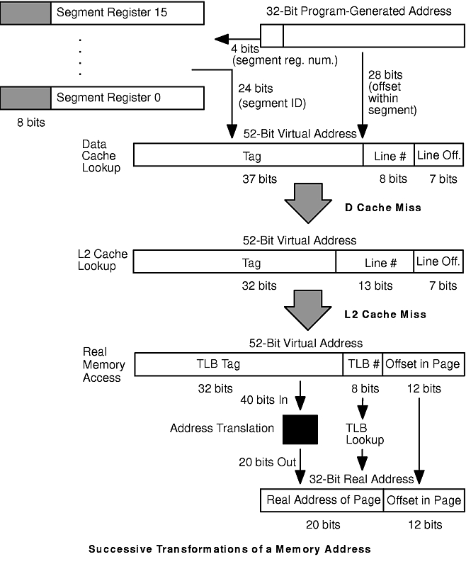
The figure "Successive Transformations of a Memory Address" in the section "Cache Lookup" shows the stages by which a 32-bit data virtual-memory address generated by a program is transformed into a real-memory address. The exact bit numbers vary by model. Models differ in detail but not in principle.
When the program requests that a register be loaded with the contents of a portion of memory, the memory location is specified by a 32-bit virtual address. The high-order 4 bits of this address are used to index into the bank of 16 segment registers. The segment registers are maintained by the operating system, and at any given time contain the 24-bit segment IDs that have been assigned to the currently executing process. Those segment IDs are unique, unless the process is sharing a segment with one or more other processes. The 24-bit segment ID from the selected segment register is combined with the 28 low-order bits of the data address to form the 52-bit virtual address of the data item to be loaded. Since the offset within the segment is 28 bits, each segment is 256MB long.
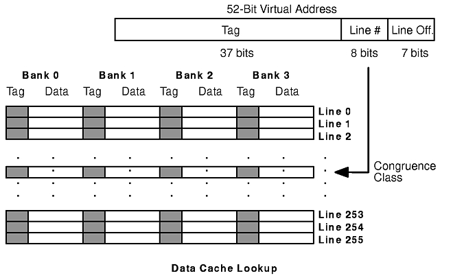
The 52-bit virtual address is used for the data cache lookup, as shown in the figure "Data Cache Lookup". Since the lines in the cache are 128 bytes long, the low-order 7 bits of the address represent the offset within the cache line. The data cache contains 128KB of space, and is four-way set associative. Thus each bank of the cache contains 256 128-byte lines (128KB/(128*4) = 256), and so the next higher-order 8 bits represent the line number (0-255). Each bank of the cache has a line with that number, and the four lines with the same number form the congruence class, that is, the four possible locations for the data being sought. This is a four-way set-associative cache. If the congruence class had two members, we would speak of the cache as two-way set-associative. If there were exactly one cache line corresponding to a given address, the cache would be direct-mapped.
Associated with each line of the cache is a 37-bit tag, which is the high-order part of the 52-bit address from which the cache line was originally loaded. If one of the tags of the four lines in the congruence set matches the high-order 37 bits of the 52-bit virtual address just generated, we have a cache hit. The data from the cache line is loaded into the register, and no access to the RAM (and so no real address) is required.
If none of the four tags in the congruence set matches the tag of the data to be loaded, there is a data cache miss. In this machine there is an L2 cache, so a cache lookup similar to the one in the data cache is performed. The primary difference between the data cache lookup and the L2 cache lookup is that the L2 is direct mapped. The lines are 128 bytes long, and the cache can hold 1MB. There are therefore 8192 lines. The low-order 7 bits of the 52-bit address are still the offset within the line. The next 13 bits constitute the cache line number. Each line is associated with a single 32-bit tag. If that tag matches the high-order 32 bits of the 52-bit address, there is an L2 cache hit. If not, the real address of the data must be determined and the data obtained from RAM.
Different implementations of the POWER architectures have different sizes and geometries of caches; some have no L2 cache, some have combined instruction and data caches, some have different line lengths. The precise size and position of the fields in the 52-bit address may differ, but the principles of cache lookup are the same.
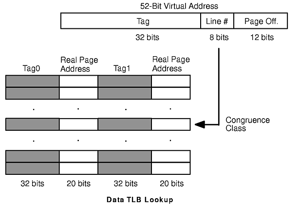
The data translation lookaside buffer (TLB) is a cache of addresses. The TLB tag is the high-order 32 bits of the 52-bit virtual address. The next 8 bits of the 52-bit virtual address are the line number in the TLB, which has 512 entries and is two-way set-associative (so each bank has 256 entries). The low-order 12 bits of the 52-bit address are the offset within the 4096-byte page. The data portion of each TLB line is the 20 high-order bits of the 32-bit real address of the page (see the figure "Data TLB Lookup"). If there is a TLB hit , the 20 high-order bits from the TLB entry are combined with the low-order 12 bits of offset within the page to form the 32-bit real address of the data.
If there is a TLB miss, the hardware determines the real address of the data using the page tables via an algorithm that is beyond the scope of this book. Obtaining the real address from the page tables takes several dozen processor cycles. When the 32-bit real address has been calculated, its 20-bit page-address portion is cached in the appropriate TLB entry, and the tag for that entry is updated appropriately.
However derived, the 32-bit real address of the data is used to issue a request to RAM. Normally, there is a latency of at least eight processor cycles between the issuing of the RAM request and the return of the first 16-byte (128 bits--the width of the memory bus) section of data, which includes the data being loaded. At this point the processor can resume operation. The RAM access continues for a further seven processor cycles to load the appropriate data cache line with its full 128 bytes, 16 bytes at a time. Thus, a cache miss entails at least 16 processor cycles from beginning to end. The tag of the cache line is updated with the high-order 37 bits of the data address. The previous content of the cache line is lost.
Several kinds of pathological addressing patterns can cause incessant cache or TLB misses, greatly slowing the effective rate of execution. For example, if the program accesses an array larger than the cache with a stride of exactly 128 bytes, it will incur a cache miss for each access. If the program presents the processor with a series of requests for the same cache line number but in different pages, a series of congruence-set collisions will occur, resulting in numerous cache misses even though the full capacity of the cache is not being used. The fact that the cache is four-way set-associative makes it unlikely that this will happen by chance, but a particularly unfortunate choice of offsets for data items could make a specific program particularly slow.
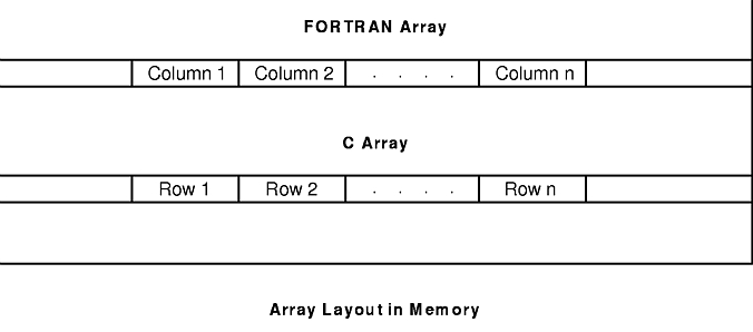
Large arrays can also cause problems. The figure "Array Layout in Memory" shows the storage layout of arrays in C and in FORTRAN. C arrays are row-major, while FORTRAN arrays are column-major. If the innermost loop of a C program indexes by column, or a FORTRAN program by row, a sufficiently large array (for example, 512x512 double-precision floating point) can cause a TLB miss on every access. For a further discussion of these phenomena, see "A (Synthetic) Cautionary Example".