84X0672 IBM PS/2 Model 25 Technical Reference, First Edition (June 1987)
Page 49-90 Physical
Text Mode Memory
Organization ?
NOTE: You
can find the Model 25 Tech Ref online, so this page is not
anything earth-shattering. I do have some further books
coming in and I -MIGHT- have some further
clarifications... I did a pin out for the 72X8300 [Video
Memory Controller] and the 72X8205
[Video Formatter], but that was SIMMply transcribing
data from the Model 30 schematics.
Programmers Guide to PC and PS/2
Video Systems: Maximum Video Performance Form the EGA,
VGA, HGC, and MCGA by Richard
Wilton
ISBN: 1556151039 / ISBN-13: 9781556151033
1st edition, Dec 01, 1987 531 pages
NOTE: The 1st edition
does a good job covering MCGA. -BUT- the second edition
['94] TOTALLY eliminates ALL MCGA info. -LFO
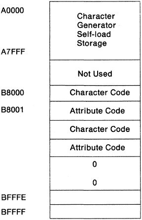
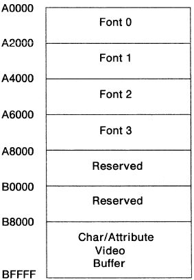
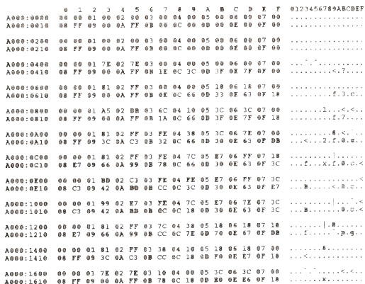
Text Mode
Memory Organization?
| Text Modes 0 - 3 |
Font Memory Map |
Layout of VRAM in A/N modes |
 |
 |
 |
Folks, I'm trying to understand why the Text Modes 0-3
does not seem to match the Font Memory Map and the Layout
of video RAM in MCGA alphanumeric modes..
What does match across all three:
A000-A800 is in use
A800-B800 is Reserved
B800-BFFF is used
Each font uses 200H [?], half for Character Code, the
other half Attribute Code. The lines for Character Code
and Attribute Code alternate
Folks, I don't understand the storing of text in RAM.
Character
Definition Tables
Like the software graphics character generators described
in Chapter 9, the hardware alphanumeric character
generator in all IBM video subsystems references a
memory-resident character definition table that contains
bit-pattern representations of the pixels in each
displayable character. Unlike the graphics-mode tables,
whose location in memory may vary, the alphanumeric tables
must lie in a predesignated portion of memory to allow the
alphanumeric character generator to access them.
Alphanumeric Character
Definitions in ROM
On the EGA, the MCGA, and the VGA, the alphanumeric
character generator uses a table of bit patterns stored in
RAM rather than in dedicated ROM. The video ROM BIOS
contains tables with which it initializes character
generator RAM whenever it establishes an alphanumeric
video mode. Because these video subsystems can set up
alphanumeric modes with different vertical resolutions,
the sizes of the default alphanumeric characters vary (see
Figure 10-1).
Alphanumeric Character
Definitions in RAM
The EGA, the VGA, the MCGA, the HGC+, and the InColor Card
all have alphanumeric character generators that use
character definition tables located in predesignated areas
of RAM. In all these subsystems, this RAM lies within the
address space of the video buffer. If you know how
character generator RAM is mapped, you can write programs
that read or update the alphanumeric character definition
tables and thereby change the displayed alphanumeric
character set.
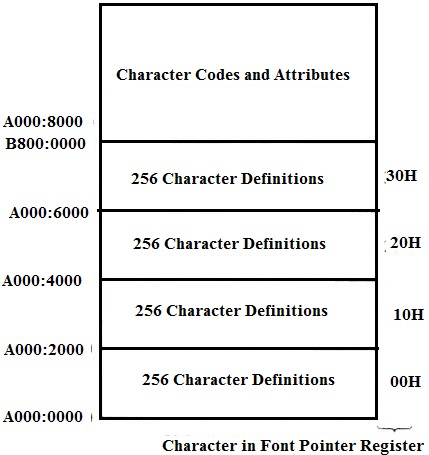
MCGA
Unlike the EGA and VGA, the MCGA has no parallel memory
maps in which to store character definitions. Instead,
alphanumeric character definitions are maintained in the
32 KB of video RAM between A000:0000 and A000:7FFF. You
can store as many as four 8 KB character definition tables
at A000:0000, A000:2000, A000:4000, and A000:6000 (see Figure 10-8).
Figure 10-8. Layout of video RAM in
MCGA alphanumeric modes.
The format of the MCGA’s character definition tables is
very different from that of any other tables discussed
thus far. Each 8 KB table is divided into 16 512-byte
lists of character codes and bit patterns (see Figure 10-9). Each list
corresponds to one scan line of the characters being
defined; the first list represents the bit patterns in the
topmost scan line of each character, the second list
corresponds to the second scan line, and so on (see Figure
10-10). Since there are 16 lists, the maximum height of a
character is 16 lines.
Figure 10-9. One of 16 lists of
character codes and bit patterns in MCGA character
generator RAM. This table defines the bit
patterns for the third scan line of each character.
Character codes are in the even-numbered bytes. The
odd-numbered bytes contain the corresponding bit patterns.
Figure 10-10. MCGA character
definitions for the first 12 scan lines of the first
16
characters. The top scan line for each
character is defined starting at A000:0000, the second
scan line starting at A000:0200, and so on. (Only the
first 32 bytes of each 512-byte list are shown.)
Updating Character Generator RAM
After you create a table of character definitions
(discussed in Chapter 9), you must make the table
accessible to the hardware character generator by properly
locating it in the video buffer. One way to do this is to
create the table in RAM (outside the video buffer) and
then copy it to character generator RAM. You can also read
the table directly from a disk file into character
generator RAM. Either technique works on any of the video
subsystems discussed here.
MCGA
As on the Hercules adapters, character generator RAM on
the MCGA is mapped linearly in the video buffer. Thus, you
can update MCGA character definitions simply by writing
the bit patterns in the appropriate format in the
character definition tables.
If you update the MCGA character definition tables
directly, however, your program must store bit patterns
and character codes in the format expected by the MCGA
character generator. It is usually better to use INT 10H
function 11H to copy character definitions into MCGA
character generator RAM. This video BIOS function
translates character definition tables from the linear
format used on the EGA and VGA into the formatted lists
used on the MCGA.
The MCGA is different from the other video subsystems
discussed here in that its alphanumeric character
generator does not fetch bit patterns from the tables at
A000:0000 as it generates characters. Instead, the
character generator uses two internal character definition
tables, called font pages. To display the characters from
one of the four tables in video RAM, you must load the
table into one of the character generator’s font pages.
Listing 10-5 shows how this is done.
Thus, displaying a new alphanumeric character set on the
MCGA is a two-step process. First, you store character
definition tables in one or more of the four 8 KB blocks
of video RAM reserved for this purpose. Then you update
the character generator’s font pages to display the
characters.
Extended Character Sets
All of the video subsystems discussed in this chapter have
enough character generator RAM to store definitions for
more than 256 characters, so they all provide a way for
the character generator to recognize extended character
codes larger than the usual eight bits.
MCGA
The MCGA supports 8-bit and 9-bit character codes with the
same BIOS interface as the EGA and VGA, although the
hardware implementation is different. On the MCGA, the two
character definition tables selected by bit 3 of a
character’s attribute byte are the ones in the MCGA’s two
internal font pages. Although you can load the font pages
by programming the MCGA’s Character Generator Interface
register (12H), Character Font Pointer register (13H), and
Number of Characters to Load register (14H), it is easier
to use INT 10H function 11H with AL = 3.
As on the EGA and VGA, bit 3 of a
character’s attribute byte does double duty as part of the
9-bit character code as well as the high-order bit of the
character’s foreground attribute. If you want to use the
same colors for both 256-character sets, you can call INT
10H function 10H to store the same set of color values in
the second eight video DAC color registers as you do in
the first eight. You can also call INT 10H function 10H to
mask bit 3 out of alphanumeric attribute decoding (see
Listing 10-8).
Changing the Displayed Character
Matrix
There is another dimension to customizing a RAM-based
character definition table: You can control the height of
the character matrix in which characters are displayed.
The height of the displayed character matrix determines
how many rows of characters appear on the screen. For
example, a 350-line display accommodates 43 rows of 8-by-8
characters but only 25 rows of 8-by-14 characters.
With all of the subsystems discussed in
this chapter, you can vary the displayed height of
alphanumeric characters by programming the CRT Controller
to display characters the same size as the characters
defined in character generator RAM. Thus, to display
8-by-8 characters on a 350-line display, you place 8-by-8
character definitions into character generator RAM and
then program the CRTC to display characters that are 8
pixels high.
MCGA
The MCGA can only display characters with 2, 4, 6, 8, 10,
12, 14, or 16 scan lines. (This is a limitation of the
MCGA’s Memory Controller.) To change the displayed
character matrix, use INT 10H function 11H to load a new
character set into the character generator. Then program
the Scan Lines per Character register (09H) with a value
from 0 through 7; if the value is n, the number of scan
lines displayed in the character matrix is (n + 1) x 2.
Listing 10-11 shows how to set up an 8-by-10 character
matrix using the MCGA’s 400-line vertical resolution to
produce 40 rows of 80 characters.
For some values in the Scan Lines per Character register,
the MCGA incorrectly displays the bottommost scan line of
the screen. Specifically, when the value in the Scan Lines
per Character register is 1, 3, 5, or 6, the MCGA
replicates part of the topmost scan line on the screen at
the bottom of the screen. Thus, you should generally avoid
using these values for the Scan Lines per Character
register.
Graphics Windows in Alphanumeric
Modes
When you update a RAM-resident character definition table,
you alter the appearance of any characters displayed using
those definitions. The contents of the displayed portion
of the video buffer need not be updated. You can exploit
this characteristic of RAM-based character definitions to
display pixel-addressable graphics images in an
alphanumeric mode, thereby displaying text with maximum
speed while including pixel-by-pixel graphics images on
the same screen.
The technique is similar on both IBM and Hercules
subsystems. Tile an area of the screen with a sequence of
characters whose attribute selects a character definition
table that contains the graphics image (see Figure 10-17). The graphics
image is created and modified by updating the appropriate
character definitions in the table. You can regard the
character definition table as a sort of virtual graphics
buffer and access individual pixels within it just as you
do in the usual graphics modes.
Figure 10-17.
A tiled graphics window in an alphanumeric mode.
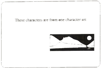
These characters are from a special character set. Each
character is one "tile"; taken together, the tiled
characters form a complete graphics image.
MCGA
Character definition tables in MCGA character generator
RAM are formatted differently than those on the EGA and
VGA, so a routine that manipulates pixels in character
generator RAM must address the tables differently (see
Listing 10-16). Also, remember that the screen does not
reflect changes to the MCGA’s character definition tables
until you load the character generator’s font pages (see
Listing 10-5).
Video
Subsystem
The video subsystem is resident on the system board and consists of:
• Video memory controller gate array
• Video formatter gate array
• 64K bytes of multi port dynamic memory
• 8K bytes static RAM character generator
• 256-by-18-bit color palette with three 6-bit digital-to-analog converters (DAC).
At the BIOS level (interrupt hex 10), the Type 8525 maintains compatibility with the IBM Color Graphics Adapter (CGA).
The video modes are compatible with those modes supported by the color graphics adapter with two modes added. The additional modes are the 320-by-200 graphics with 256 colors available and the 640-by-480 graphics with two colors available.
Block Diagram
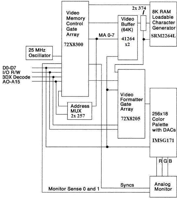
Figure 1-21. Video Subsystem Block
Diagram
NOTE: The 25/30 only
use two Monitor Sense lines, MS0 [pin 11] and MS1 [pin
12]. The pins for Monitor ID3 [pin 15] and Monitor ID2
[pin 4] are N/C on the 25/30. -LFO
Display Support
The video subsystem supports a 31.5 kHz analog color display or 31.5 kHz analog monochrome display. The system senses the type of display and matches the initialization to it. The polarity of the vertical synchronization signal to the display determines the number of horizontal scans, either 400 or 480. The number of scan lines in relation to the polarity is:
|
Scan
Lines |
Vertical
Sync |
Horizontal
Sync |
|
480 |
Negative |
Negative |
|
400 |
Positive |
Negative |
If
the system senses the presence of a monochrome display, it
sums the colors and outputs the video signal to pin 4
(green) of the video connector on the system board.
NOTE: Using only one color
gun results in a sharper picture on CRTs, as there is no
possibility of convergence error. I can't prove it, but an
LCD wouldn't have a convergence issue -LFO
Text Modes
In the text modes, the character box size is 8-by-16. The character font table is loaded into the character generator. All 16 scan lines are programmed into the character generator.
Graphics Modes
In the graphics modes, the character font table is used to create the character PELs. For most graphics modes, the character box is an 8-by-8 character box that is double-scanned to create an 8-by-16 character; however, all 16 scan lines of the 8-by-16 box are not programmable. The 640-by-480 graphics mode is the exception. It uses an 8-by-16 character box and a separate font table. In this mode, 30 character rows are displayed.
Figure 1-22. Video Mode Summary
|
Video
Modes |
Analog
Display |
|
Mode
0,1 40
Column Alphanumeric |
40
column by 25 rows 8-by-16
character box 320
by 400 16
of 256K colors or 16 of 64 shades of gray
(monochrome) Display
buffer B8000 2000
byte video buffer |
|
Mode
2,3 80
Column Alphanumeric |
80
column by 25 rows 8-by-16
character box 640
by 400 16
of 256K colors or 16 of 64 shades of gray
(monochrome) Display
buffer B8000 4000
byte video buffer |
|
Mode
4,5 320
by 200 Graphics |
8-by-8
character box Double-scanned 320
by 200 4 of
256K colors or 4 of 64 shades of gray
(monochrome) Alternate
palette select Display
buffer B8000 16000
byte video buffer Two
row scan address partitions |
|
Mode
6 640
by 200 Graphics |
8-by-8
character box Double-scanned 640
by 200 2 of
256K colors Display
buffer B8000 16000
byte video buffer Two
row scan address partitions |
|
Mode
11 640
by 480 Graphics |
8-by-16
character box 640
by 480 2 of
256K colors Display
buffer A0000 38400
byte video buffer Linear
addressing |
|
Mode
13 320
by 200 Graphics |
8-by-8
character box Double-scanned 320
by 200 256
of 256K colors Display
buffer A0000 64000
byte video buffer Linear
addressing |
Display Formats
In alphanumeric (text) modes 0 through 3, two bytes define each character on the display screen. The even byte accesses the character generator to create the PEL data. The odd byte defines the color of the PELs. Sixteen colors are available for foreground, and eight colors are available for background when blink is enabled (default). Blink is controlled in the EGA Mode Control register, hex 3D8. The format of the two bytes is shown in the following:
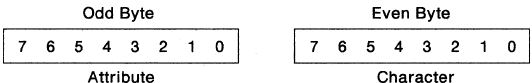
Figure 1-23. Alphanumeric Format
The following are the bit definitions of the attribute byte. Bit 7 selects a blinking character, or if blinking is disabled, selects palette addresses above hex 07 for the background color.
Figure 1-24. Attribute Byte
|
Bits |
Function |
|
7
to 4 |
Background
Color Palette Address |
|
3
to 0 |
Foreground
Color Palette Address |
In modes 4 and 5, the bit pair C1 and C0 selects one of four colors for each PEL.
Figure 1-25. Modes 4 and 5
|
Bit |
PEL
Definition |
|
|
7,6 |
C1,C0 |
First
PEL |
|
5,4 |
C1,C0 |
|
|
3,2 |
C1,C0 |
|
|
1,0 |
C1,C0 |
Last
PEL |
There are two color sets: color set 0 and color set 1. For information about the colors selected, see "CGA Border Control Register, 3D9," later in this section under "Video Formatter Registers."
In modes 6 and 11, one bit defines each PEL, with the most significant bit defining the first PEL. The foreground color maps to the color in the CGA Border Control register if the B&W bit in the CGA Mode Control Register is 0. If the B&W bit is 1, the foreground color maps to palette address hex 07. The background color always maps to address hex 00.
Figure 1-26. Modes 6 and 11
|
Bit |
PEL
Definition |
|
|
7 |
C0 |
First
PEL |
|
6 |
C0 |
|
|
5 |
C0 |
|
|
4 |
C0 |
|
|
3 |
C0 |
|
|
2 |
C0 |
|
|
1 |
C0 |
|
|
0 |
C0 |
Last
PEL |
In mode 13, a byte defines each PEL. This allows a choice of 256 colors for each PEL.
Video Storage Organization
The following is the memory mapping for text modes 0 through 3.
Figure 1-27. Text Modes 0 through 3
The following is the memory mapping for graphics modes 4 through 6. In modes 4 and 5, each byte defines four PELs. In mode 6, each byte defines eight PELs.
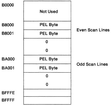
Figure 1-28. Graphics Modes 4 through 6
The following is the memory
mapping for graphics modes 11 and 13. In mode 11, each
byte defines eight PELs; in mode 13, each byte defines
one PEL.
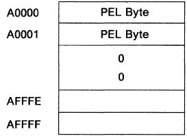
Figure 1-29. Graphics Modes 11 and 13
Video Registers
The video memory controller gate array responds to I/O addresses 3D4 and 3D5. The video formatter gate array responds to I/O addresses 3D8 through 3DF.
The color palette is programmed through the video formatter at addresses 3C6 through 3C9. All registers are readable.
The following pages describe the memory controller registers, the video formatter registers, the color palette registers, and the character generator. Sample programs of a font load and palette load are also included.
Video Memory Controller Registers
The video memory controller contains an index register and 22 data registers. Two I/O commands are required to write to one data register: writing the desired index value to address hex 3D4, and then writing the data to address hex 3D5.
Memory Controller Index Register, Hex 3D4: This register is read/write, and points to the specific data register addressed through hex 3D5.
Figure 1-30. Video Memory Controller
Index Register
|
Bit |
Function |
|
7 |
Reserved |
|
6 |
Reserved |
|
5 |
Index5 |
|
4 |
Index4 |
|
3 |
Index3 |
|
2 |
Index2 |
|
1 |
Index1 |
|
0 |
Index0 |
The following is a list of the 22 data registers and their functions.
|
Index
(Hex) |
Register
Description |
|
00 |
Horizontal
Total |
|
01 |
Horizontal
Characters Displayed |
|
02 |
Start
Horizontal Sync |
|
03 |
Sync
Pulse Width |
|
04 |
Vertical
Total |
|
05 |
Vertical
Total Adjust |
|
06 |
Vertical
Characters Displayed |
|
07 |
Start
Vertical Sync |
|
08 |
Reserved |
|
09 |
Scan
Lines per Character |
|
0A |
Cursor
Start |
|
0B |
Cursor
End |
|
0C |
Start
of Screen High |
|
0D |
Start
of Screen Low |
|
0E |
Cursor
Position High |
|
0F |
Cursor
Position Low |
|
10 |
Mode
Control |
|
11 |
Interrupt
Control |
|
12 |
Character
Generator Interface and Sync Polarity, or
Display Sense |
|
13 |
Character
Font Pointer |
|
14 |
Number
of Characters to Load |
|
20 |
Reserved |
Horizontal Total Register, Index 00: This register contains the total number of characters in the horizontal scan interval. The number consists of both displayed and nondisplayed characters. This register determines the frequency of the 'horizontal sync' signal.
Horizontal Characters Displayed Register, Index 01: This register determines the total number of characters to be displayed during the horizontal video scan interval. This register is loaded with a value of hex 27. The hardware calculates the correct value based on the mode selected.
Start Horizontal Sync Register, Index 02: This register specifies the character position count at which the 'horizontal sync' signal becomes active.
Sync Pulse Width Register, Index 03: This register specifies the pulse widths of the horizontal and vertical synchronization signals. The horizontal pulse width is programmed in units of character clocks. The vertical pulse width is programmed in units of the horizontal synchronization period. This register is programmed to match the display specifications.
Figure 1-31. Sync Pulse Width Register
|
Bit |
Function |
|
7 |
Width
VSync3 |
|
6 |
VSync2 |
|
5 |
VSync1 |
|
4 |
VSync0 |
|
3 |
Width
HSync3 |
|
2 |
HSync2 |
|
1 |
HSync1 |
|
0 |
HSync0 |
Vertical Total Register, Index 04: This register contains the 8 least significant bits for the total number of scan lines in the vertical scan interval. The most significant bit is the inversion of bit 6 of the Mode Control register. The total number consists of both the displayed and nondisplayed scan lines. This register and the Vertical Total Adjust register determine the frequency of the 'vertical sync' signal.
Vertical Total Adjust Register, Index 05: This register is used to adjust the total number of horizontal scan lines in the vertical scanning interval. It allows for an odd number of horizontal lines (525 for 60 Hz). The minimum value for this register is hex 02.
Figure 1-32. Vertical Total Adjust
Register
|
Bit |
Function |
|
7 |
Reserved |
|
6 |
Reserved |
|
5 |
VAdjust5 |
|
4 |
VAdjust4 |
|
3 |
VAdjust3 |
|
2 |
VAdjust2 |
|
1 |
VAdjust1 |
|
0 |
VAdjust0 |
Vertical Characters Displayed Register, Index 06: This register contains the 8 least significant bits for the number of scan lines displayed in the vertical scan interval. The most significant bit is the inversion of bit 6 of the Mode Control register.
Start Vertical Sync Register, Index 07: This register contains the 8 least significant bits for the vertical scan line count. It determines when the 'vertical sync' signal becomes active. The most significant bit is the inversion of bit 6 of the Mode Control register.
Scan Lines per Character Register, Index 09: This register determines the number of horizontal scan lines in a character row. In text modes, the value is hex 07. In graphics modes 4 through 6, the value is hex 01, and in modes 11 and 13, the value is hex 00. The hardware calculates the proper value based on the mode selected.
Figure 1-33. Scan Lines per Character
Register
|
Bit |
Function |
|
7 |
Reserved |
|
6 |
Reserved |
|
5 |
Reserved |
|
4 |
Reserved |
|
3 |
Row
Size3 |
|
2 |
Row
Size2 |
|
1 |
Row
Size1 |
|
0 |
RowSize0 |
Cursor Start Register, Index 0A: Bits 3 through 0 in this register determine the horizontal scan line count at which the cursor output becomes active. The value in this register should be lower than the value in the Cursor End register. The minimum is 0. The hardware will double-scan the cursor to produce the proper cursor display for a 16-scan-line character box.
When bit 5 is 1, the cursor is not displayed.
Figure 1-34. Cursor Start Register
|
Bit |
Function |
|
7 |
Reserved |
|
6 |
Reserved |
|
5 |
Blank
Cursor |
|
4 |
Reserved |
|
3 |
Cursor
Start3 |
|
2 |
Cursor
Start2 |
|
1 |
Cursor
Start1 |
|
0 |
Cursor
Start0 |
Cursor End Register, Index 08: This register determines the horizontal scan line count when the cursor output becomes inactive. The value should be greater than the value in the Cursor Start register. The maximum is 7.
Figure 1-35. Cursor End Register
|
Bit |
Function |
|
7 |
Reserved |
|
6 |
Reserved |
|
5 |
Reserved |
|
4 |
Reserved |
|
3 |
Cursor
End3 |
|
2 |
Cursor
End2 |
|
1 |
Cursor
End1 |
|
0 |
Cursor
End0 |
Start of Screen High Register,
Index
0C: This register contains the 8 most
significant bits for the starting memory address of the
video display buffer. Sixteen address bits determine the
starting address.
This register is initialized to a value of hex 00.
Start of Screen Low Register, Index 0D: This register, together with the Start of Screen High register, gives the starting address of the display buffer. For all modes, this register is initialized to a value of hex 00.
Cursor Position High Register, Index 0E: This register contains the four most significant bits for the cursor location.
Figure 1-36. Cursor Position High
Register
|
Bit |
Function |
|
7 |
Reserved |
|
6 |
Reserved |
|
5 |
Reserved |
|
4 |
Reserved |
|
3 |
Cursor
PositionB |
|
2 |
Cursor
PositionA |
|
1 |
Cursor
Position9 |
|
0 |
Cursor
Position8 |
Cursor Position Low Register, Index 0F: This register contains the eight least significant bits for the location of the cursor. A value of hex 00 in both of these registers will locate the cursor in the upper left corner. The cursor is not supported in any graphics mode.
Mode Control Register, Index 10: Writing to this register selects the type of display and clock times, and selects some of the graphics modes.
Figure 1-37. Mode Control, Write
|
Bit |
Function |
|
7 |
Inhibit
Write |
|
6 |
Reserved
= 0 |
|
5 |
Reserved |
|
4 |
Clock
= 1 -OR- 0 |
|
3 |
Compatibility |
|
2 |
Reserved |
|
1 |
Mode
11 |
|
0 |
256
Color |
Write
Bit 7 When set to 1, the
Inhibit Write bit prevents any writes to the horizontal
and vertical registers. After a mode set, BIOS sets this
bit to 1 to prevent applications designed for other color
graphics adapters from altering those registers.
NOTE: When Bit 7 is set to
1, registers 00H-07H are set to "Read Only" so that
horizontal
and vertical timing parameters are not inadvertently
disrupted.
Bit 6 The inverse of this bit is used as the ninth bit of the vertical compare circuits and must be set to 0.
Bit 5 Reserved.
Bit 4 This bit selects the
dot clock and must be set to 1 [25.175 MHz]
NOTE: TubeTimeUS has
determined 0 [14.318 MHz] is valid.
Bit 3 When set to 1, this bit allows the circuitry to calculate the correct horizontal register values for the 80-by-25 text modes. This bit should be set to 1 for all modes.
Bit 2 Reserved.
Bit 1 When set to 1, this bit selects mode 11.
Bit 0 When set to 1, this bit selects mode 13. Bit 2 in the Extended Mode Control register must also be set.
During certain operations, the circuitry calculates some of the internal signals and returns the values to the Mode Control register.
Figure 1-38. Mode Control, Read
|
Bit |
Function |
|
7 |
80x25 |
|
6 |
Reserved |
|
5 |
Clock
Select |
|
4 |
Clock
= 1 -OR- 0 |
|
3 |
Alpha
Mode |
|
2 |
Double-Scan |
|
1 |
Mode
11 |
|
0 |
Mode
13 |
Read
Bit 7 This bit indicates the state of bit 0 in the CGA Mode Control register. When set to 1, this bit indicates that 80-by-25 mode is selected.
Bit 6 Reserved.
Bit 5 When this bit is 1, it indicates that the clock is not divided by 2, and the resolution is 640 PELs wide. When it is 0, the resolution is 320.
Bit 4 When this bit is 1,
it indicates that the dot clock is 25.175 MHz.
NOTE: TubeTimeUS has
determined 0 [14.318 MHz] is valid.
Bit 3 When set to 1, this bit indicates that the mode is a text mode.
Bit 2 When set to 1, this bit indicates that the scan lines are double-scanned.
Bit 1 When set to 1, this bit indicates that mode 11 is selected.
Bit 0 When set to 1, this bit indicates that mode 13 is selected.
Interrupt Control Register, Index 11: This register controls IRQ2 output to the interrupt controller. It also shows the status of the interrupt. The output drivers are tri-stated (bit 7) to allow a Read of the Display Sense register.
Figure 1-39. Interrupt Control Register
|
Bit |
Function |
|
7 |
Tri-State
Output |
|
6 |
IRQ2
Status |
|
5 |
-Enable
IRQ2 |
|
4 |
-Clear
IRQ2 Latch |
|
3 |
Reserved |
|
2 |
Reserved |
|
1 |
Reserved |
|
0 |
Reserved |
Bit 7 When set to 1, this bit disables (tri-states) the output drivers and selects the Display Sense register to be read at index 12 instead of the Character Generator Interface and Sync Polarity register.
Bit 6 When set to 1, this bit indicates that the memory controller is causing an interrupt. This bit is read-only.
Bit 5 When cleared to 0, this bit enables the interrupt.
Bit 4 When cleared to 0, this bit holds the interrupt latch clear.
Bits 3-0 These bits are reserved and should be 0.
Character Generator Interlace and Sync Polarity Register, Index 12: This register controls the character font tables and the horizontal and vertical synchronization signals, HSYNC and VSYNC. To read this register, bit 7 of the Interrupt Control register must be 0.
Figure 1-40. Character Generator
Interface and Sync Polarity Register
|
Bit |
Function |
|
7 |
Load
Character Generator |
|
6 |
Load
Full Character Set |
|
5 |
Swap
Active Font |
|
4 |
Enable
512 Characters |
|
3 |
Reserved
= 0 |
|
2 |
Enable
Sync Outputs |
|
1 |
VSYNC
Polarity |
|
0 |
HSYNC
Polarity |
Bit 7 When written as a 1, this bit loads the character generator. When read as a 0, the bit indicates that the load has finished. To start the load, this bit is first cleared and then set to 1.
Bit 6 When set to 1, this bit causes the character generator to load the display memory during normal display time. When clear, the display memory is loaded only during the vertical blanking interval.
Bit 5 This bit selects the font page that is used as font table or that the character generat9r loads. When set to 1, font page 1 is selected; when cleared to 0, font page 0 is selected.
Bit 4 When this bit is set to 1, 512 character codes are displayable in the text modes. Bit 3 of the attribute byte then determines the font page when displaying the character. When this bit is set to 1, only eight foreground colors are supported. When this bit is cleared to 0, only 256 character codes are displayed, and bit 5 of this register determines the active font.
Bit 3 Reserved = 0.
Bit 2 When set to 1, this bit enables HSYNC and VSYNC outputs to the display.
Bit 1 When set to 1, this bit causes VSYNC to be positive polarity.
Bit 0 When set to 1, this bit causes HSYNC to be positive polarity.
Display Sense Register, Index 12: This register contains the sensed levels of the monitor sense 1 and 0 signals at pins 13 and 14 of the display connector. This information is used by BIOS to properly initialize all video registers to match the display. To read this register, bit 7 of the Interrupt Control register is set to 1.
These levels are used to determine the type of display attached as shown in the following. The bit is set when the polarity is positive.
Figure 1-41. Monitor Sense Bits
|
Sense
1 |
Sense
0 |
Type
of Display Attached |
|
Bit
1 |
Bit
0 |
|
|
0 |
0 |
Reserved |
|
0 |
1 |
Analog
Monochrome Display |
|
1 |
0 |
Analog
Color Display |
|
1 |
1 |
No
Display Attached |
Character Font Pointer Register, Index 13: This register contains a pointer to the character font table. The only valid pointer values are hex 00, 10, 20, or 30. The pointer value doubled and the hex value A0000 make up the segment for the font table. The character value doubled is the offset into the table. See "RAM-Loadable Fonts," later in this section.
Number of Characters to Load Register, Index 14: This register determines the number of characters to load into the RAM-loadable character generator during one vertical retrace interval. This register is used only in the text modes.
Video Formatter Registers
The video formatter registers at I/O addresses hex 3D8 and 3D9 duplicate the functions of the 6845 registers in the color graphics adapter. Registers are added at addresses hex 3DD through 3DF for Type 8525 initialization requirements. The video formatter registers at addresses hex 3C6 through 3C9 control the color palette.
Register
Description
3D8 CGA Mode Control
3D9 CGA Border Control
3DA CGA Status
3DB Reserved
3DC Reserved
3D0 Extended Mode Control
3DE Reserved
3DF Reserved
3C6 PEL Mask
3C7 Palette Read Address
3C8 Color Palette Address
3C9 Color Palette Data
CGA Mode Control Register, 3D8: This register contains the mode control information for color/graphics compatible functions.
|
Bits 7,6 |
Reserved. |
|
Bit 5 |
When set to 1, this bit selects
the blink option for text modes. When cleared to
0, 16 background colors are available in the text
modes. |
|
Bit 4 |
When set to 1, this bit selects
mode 6, 640-by-200 double scanned graphics. |
|
Bit 3 |
When set to 1, this bit enables
display image. |
|
Bit 2 |
When bit is 1, palette
addresses hex 00 and 07 are the two colors used in
modes 6 and 11. When bit is 0, address hex 00 and
the address specified in the CGA Border Control
register are the two colors used. |
|
Bit 1 |
When set to 1, this selects
modes 4 and 5, 320-by-200 double-scanned graphics. |
|
Bit 0 |
When set to 1, this bit selects
the 80-by-25 text mode. |
Figure 1-42. CGA Mode Register
|
Bit |
Function |
|
7 |
Reserved |
|
6 |
Reserved |
|
5 |
Enable
Blink |
|
4 |
640-by-200
Mono |
|
3 |
Enable
Video |
|
2 |
B&W |
|
1 |
Graphics |
|
0 |
80-by-25
Alpha |
CGA Border Control Register, 3D9: This register contains the border color information and selects the alternate color palette for modes 4 and 5. Although analog displays do not have borders, the border color information selects the alternate foreground color for modes 6 and 11, and the background color for modes 4 and 5.
Figure 1-43. CGA Border Control
Register
|
Bit |
Function |
|
7 |
Reserved |
|
6 |
Reserved |
|
5 |
320-by-200
Palette Select |
|
4 |
Alternate
Intensity |
|
3
to 0 |
Border
Color |
Bits 7,6 Reserved
Bit 5 When set to 1, this bit selects color set 1 for modes 4 and 5.
Bit 4 When set to 1 (default), this bit selects an intensified color set for modes 4 and 5.
Bits 3-0 These bits select the palette address for the border color information used by modes 4, 5, 6, and 11.
The following figure shows the effects of this register and the bit pair C1,C0 and how the two color sets map into the color palette.
Figure 1-44. Modes 4 and 5 Color
Selection
|
BCR
Bit 4 |
C1 |
C0 |
BCR
Bit 5 |
Palette
Address |
|
X |
0 |
0 |
X |
Background
Color |
|
0 |
0 |
1 |
0 |
02
Color Set 0 |
|
0 |
1 |
0 |
0 |
04
Color Set 0 |
|
0 |
1 |
1 |
0 |
06
Color Set 0 |
|
0 |
0 |
1 |
1 |
03
Color Set 1 |
|
0 |
1 |
0 |
1 |
05
Color Set 1 |
|
0 |
1 |
1 |
1 |
07
Color Set 1 |
|
|
|
|
|
Intensified
Colors |
|
1 |
0 |
1 |
0 |
0A
Color Set 0 |
|
1 |
1 |
0 |
0 |
0C
Color Set 0 |
|
1 |
1 |
1 |
0 |
0E
Color Set 0 |
|
1 |
0 |
1 |
1 |
0B
Color Set 1 |
|
1 |
1 |
0 |
1 |
0D
Color Set 1 |
|
1 |
1 |
1 |
1 |
0F
Color Set 1 |
CGA Status Register, 3DA: This register is read-only and contains the status information for the color graphics adapter.
Figure 1-45. Status Register
|
Bit |
Function |
|
7 |
Reserved |
|
6 |
Reserved |
|
5 |
Reserved |
|
4 |
Reserved |
|
3 |
Vertical
Sync |
|
2 |
Reserved |
|
1 |
Reserved |
|
0 |
-Display
Enable |
Extended Mode Control Register, 3DD: This register controls the selection of the type of display and the advanced color support. When cleared to 0, bit 7 indicates that a readable DAC is installed; when set, it indicates that the DAC is not a readable type. Bit 2 must be set to 1 to select mode 13.
Figure 1-46. Extended Mode Control
Register
|
Bit |
Function |
|
7 |
-Readable
DAC Installed |
|
6 |
Reserved |
|
5 |
Reserved |
|
4 |
Reserved |
|
3 |
Reserved |
|
2 |
256
Colors |
|
1 |
Reserved |
|
0 |
Reserved
= 0 |
Color Palette Registers
Three registers are used to access the color palette: a mask register, a read address register, and a write address register.
The color palette has 256 18-bit data registers and an 8-bit address register. Each data register is divided into three 6-bit data areas, one for each color. To load each data register takes three outputs in the sequence of red, green, blue.
When accessing the palette, the interrupts should be disabled to prevent the sequence from being interrupted. The palette supports both a single-register write operation and a burst load operation.
To maintain software compatibility, programmers should use the BIOS interface when loading the color palette. BIOS supports two calls for setting and two calls for reading the color registers. The calls are through interrupt 10H with (AH) = hex 10. The value in the AL register determines the specific operation:
10 - Set individual color register
12 - Set block of color registers
15 - Read individual color register
17 - Read block of color registers
Single Register Load: The address for the specific color register (0 - 255) is loaded into the BX register. The DH, CH, and CL registers contain the red, green, and blue values, respectively. In the following example using the BIOS interface, the yellow color value is loaded into the palette address normally assigned to white. If the Set Mode call has been initialized to restore the color palette to its default state, the mode must be set before changing the color palette.
;-----Set
up the video mode
MOV
AX,0004H ;
Set mode to mode 4
INT 10H
; Video BIOS interrupt
;-----Read
color 14 to get the red, green, and blue values for
yellow
MOV
AX,1015H ;
Read individual color register
MOV BX,0EH
;
Read color register 0EH
INT 10H ;
Video BIOS interrupt
;
Return with DH = red value
;
CH = green value
;
CL = blue value
;-----Set
color 15 to the red, green, and blue values of yellow
MOV
AX,1010H ;
Set individual color register
MOV BX,0FH ;
Set color register 0FH
INT 10H
; Video BIOS interrupt
Burst Load: This second call supports setting a block of color registers. Using this call, 1 to 256 color values can be set or read with a single BIOS call. The BX register contains the address for the first register to be set, and CX contains the number of registers. ES:DX point to a table of color values, where each table entry contains the red, green, and blue values for a color. The following example sets the first 16 colors in the color palette.
;-----Set
colors 0 thru 15 with a set block of color registers
call
CODE SEGMENT
'CODE'
ASSUME
CS:CODE, ES:NOTHING, OS:NOTHING
SET_BLK_EX
PROC FAR
PUSH DS
XOR AX.AX
PUSH AX
;
Return address for DOS
PUSH CS
POP ES
;
Establish ES addressing for table
MOV AX,
1012H ; Set
block of color register call
MOV BX, 0
;
Start with color 0
MOV CX, 16
;
Set 16 color registers
MOV DX,
OFFSET CLR_TABLE ;
ES:DX point to color table
INT 10H
;
Make the video BIOS interrupt
RET
SET_BLK_EX
ENDP
CLR_TABLE
LABEL BYTE
DB
00H,00H,00H
; Black 00
DB
00H,00H,2AH
; Blue 01
DB
00H,2AH,00H
; Green
02
DB
00H,2AH,2AH
; Cyan 03
DB
2AH,00H,00H
;
Red 04
DB
2AH,00H,2AH
; Magenta
05
DB
2AH,15H,00H
; Brown 06
DB
2AH,2AH,2AH
; White 07
DB
15H,15H,15H
; Gray 08
DB
15H,15H,3FH
; Lt blue
09
DB
15H,3FH,15H
; Lt green
0A
DB
15H,3FH,3FH
; Lt cyan
08
DB
3FH,15H,15H
; Lt red 0C
DB
3FH,15H,3FH
; Lt magenta
0D
DB
3FH,3FH,15H
; Lt yellow 0E
DB
3FH,3FH,3FH
; Bright White
0F
CODE ENDS
END
PEL Mask Register, 3C6: This register is initialized to a value that does not affect the color selection, hex FF. This value should not be changed because mask operations are not supported on the Type 8525.
Palette Read Address Register, 3C7: This register contains the pointer to one of 256 palette data registers and is used when reading the color palette.
Reading this port returns the last command cycle to the palette. The description of bits 1 and 0 is in the following table. All other bits during a read of this port are reserved.
Figure 1-47. Last
Palette Command
|
Bit
1 |
Bit
0 |
Last
Palette Command |
|
0 |
0 |
Write
Palette Cycle |
|
0 |
1 |
Reserved |
|
1 |
0 |
Reserved |
|
1 |
1 |
Read Palette
Cycle |
Color Palette Address Register, 3C8: This register contains the pointer to one of 256 palette data registers and is used during a palette load.
Color Palette Data Register, 3C9: This register contains a 6-bit value that yields one of 64 color levels. To write a color, the address is loaded into the Color Palette Address register. Three writes to this register are needed for each palette address: the first is the red color information, the second is the green, and the third is the blue.
To read a color, the address value is written to the Palette Read Address register, followed by three reads of this register. The first returns the red color information, the second returns the green, and the third returns the blue.
Figure 1-48. Color Palette Data Register
|
Bit |
Function |
|
7 |
Not
Used |
|
6 |
Not
Used |
|
5 |
PD
5 |
|
4 |
PD
4 |
|
3 |
PD
3 |
|
2 |
PD
2 |
|
1 |
PD
1 |
|
0 |
PD
0 |
Video Initialization Tables
The following figures show the video register values used by BIOS for the various display modes.
Figure 1-49. Memory Controller
Initialization
|
Index Pointer |
Data
Register Description |
0,1 |
2,3 |
4,5 |
6 |
11 |
13 |
|
00 |
Horz.
Total |
30 |
30 |
30 |
30 |
30 |
30 |
|
01 |
Horz.
Displayed |
27 |
27 |
27 |
27 |
27 |
27 |
|
02 |
Start
Horz. Sync |
2A |
2A |
2A |
2A |
2A |
2A |
|
03 |
Sync
Pulse Width |
26 |
26 |
26 |
26 |
26 |
26 |
|
04 |
Vert.
Total |
80 |
80 |
80 |
80 |
FF |
80 |
|
05 |
Vert.
Adjust |
00 |
00 |
00 |
00 |
0A |
00 |
|
06 |
Vert.
Displayed |
8F |
8F |
8F |
8F |
0F |
8F |
|
07 |
Start
Vert. Sync |
98 |
98 |
98 |
98 |
E9 |
9B |
|
08 |
Reserved |
XX |
XX |
XX |
XX |
XX |
XX |
|
09 |
Char.
Scan Lines |
07 |
07 |
01 |
01 |
00 |
00 |
|
0A |
Cursor
Scan Start |
06 |
06 |
XX |
XX |
XX |
XX |
|
0B |
Cursor
Scan End |
07 |
07 |
XX |
XX |
XX |
XX |
|
0C |
Start
of Screen (High) |
00 |
00 |
00 |
00 |
00 |
00 |
|
0D |
Start
of Screen (Low) |
00 |
00 |
00 |
00 |
00 |
00 |
|
0E |
Cursor
Position (High) |
00 |
00 |
XX |
XX |
XX |
XX |
|
0F |
Cursor
Position (Low) |
00 |
00 |
XX |
XX |
XX |
XX |
|
10 |
Mode
Control |
18 |
18 |
18 |
18 |
1A |
19 |
|
11 |
Interrupt
Control |
30 |
30 |
30 |
30 |
30 |
30 |
|
12 |
Char.
Gen/Sync Pol. |
46 |
46 |
46 |
46 |
04 |
46 |
|
13 |
Char.
Font Pointer |
00 |
00 |
XX |
XX |
XX |
XX |
|
14 |
Char.
to Load |
FF |
FF |
XX |
XX |
XX |
XX |
Figure 1-50. Video Formatter
Initialization Table
|
|
|
Modes |
|||||
|
Address |
Data
Register Description |
0 |
1
2 |
3
4 |
5
6 |
11 |
13 |
|
3C6 |
PEL
Mask |
FF |
FF |
FF |
FF |
FF |
FF |
|
3D8 |
CGA
Mode Control |
28 |
29 |
0A |
18 |
18 |
08 |
|
3D9 |
CGA
Border Control |
30 |
30 |
30 |
3F |
3F |
30 |
|
3DA |
Status |
XX |
XX |
XX |
XX |
XX |
XX |
|
3DB |
Reserved |
XX |
XX |
XX |
XX |
XX |
XX |
|
3DC |
Reserved |
XX |
XX |
XX |
XX |
XX |
XX |
|
3DD |
Extended
Mode Control |
00 |
00 |
00 |
00 |
00 |
04 |
|
3DE |
Reserved |
|
|
|
|
|
|
|
3DF |
Reserved |
|
|
|
|
|
|
Figure 1-51. 16-Color Compatibility
Initialization
|
3C8 |
|
3C9 |
|
|
|
Index |
R |
G |
B |
Display
Color |
|
00 |
00 |
00 |
00 |
Black |
|
01 |
00 |
00 |
2A |
Blue |
|
02 |
00 |
2A |
00 |
Green |
|
03 |
00 |
2A |
2A |
Cyan |
|
04 |
2A |
00 |
00 |
Red |
|
05 |
2A |
00 |
2A |
Magenta |
|
06 |
2A |
15 |
00 |
Brown |
|
07 |
2A |
2A |
2A |
White |
|
08 |
15 |
15 |
15 |
Gray |
|
09 |
15 |
15 |
3F |
Light
Blue |
|
0A |
15 |
3F |
15 |
Light
Green |
|
0B |
15 |
3F |
3F |
Light
Cyan |
|
0C |
3F |
15 |
15 |
Light
Red |
|
00 |
3F |
15 |
3F |
Light
Magenta |
|
0E |
3F |
3F |
15 |
Yellow |
|
0F |
3F |
3F |
3F |
Bright
White |
RAM-Loadable Fonts
In the text modes, the video buffer is divided into two data areas: the text area at address B8000 and the character font tables at address A0000. The text area consists of the character and attribute code for each position on the display. The font table consists of the character code and PEL data for each character in the set.
Restrictions are placed on where the character font can be loaded into the video buffer. Four fonts are supported in text modes. The memory map below shows the areas (blocks) in the video buffer where the fonts are loaded. The font tables can be swapped in synchronization with the 'vertical retrace' signal with several output commands. A maximum of four fonts can be loaded into the font area, but only two can be loaded into and displayed from the character generator at anyone time. Two fonts are provided in ROM, an 8-by-8 font and an 8-by-16 font. The font loaded depends on the mode that is active at the time.
Figure 1-52. Font Memory Map
The following is an example of how the character "E" is defined in an 8-by-16 character box.
Figure 1-53. Sample Character
|
Scan
Line |
Data
in Hex |
Data
in Binary |
|
0 |
00 |
00000000 |
|
1 |
00 |
00000000 |
|
2 |
7E |
01111110 |
|
3 |
7E |
01111110 |
|
4 |
60 |
01100000 |
|
5 |
60 |
01100000 |
|
6 |
7E |
01111110 |
|
7 |
7E |
01111110 |
|
8 |
60 |
01100000 |
|
9 |
60 |
01100000 |
|
10 |
7E |
01111110 |
|
11 |
7E |
01111110 |
|
12 |
00 |
00000000 |
|
13 |
00 |
00000000 |
|
14 |
00 |
00000000 |
|
15 |
00 |
00000000 |
The following programming example uses the BIOS routine to load a font table into block 0. Because of differences in the hardware, the character generator is not loaded the same for all display adapters; however, the BIOS routines are the same for all video subsystems with RAM-loadable fonts. The Type 8525, for instance, supports only 8-by-8 and 8-by-16 character fonts, depending on the mode selected.
TITLE Load
block 0 with character definitions from "SET_A"
CODE SEGMENT
PARA 'CODE'
ASSUME
CS:CODE,ES:CODE
EXl PROC NEAR
MOV
AX,000lH
; Mode set BIOS call for mode 1
INT
l0H;
MOV
CX,100H
; Load 256 characters into the block
MOV
DX,0000H
; Begin loading at offset zero
MOV
BL,00H
; Load the characters into block zero
MOV
BH,10H
; 16 bytes per character definition
MOV
AX,SEG SET_A
; Get the segment of the characters
MOV
ES,AX
; ES = segment of character definitions
MOV
AH,11H
; Character generator routines
MOV
AL,00H
; User alpha load BIOS call
MOV
BP,OFFSET SET_A ;
BP = offset of character definitions
INT
l0H
RET
EXl ENDP
;----8-by-16
definitions for "SET_A"
SET_A LABEL
BYTE
INCLUDE SET_A_CHARS
SET_A_END EQU $
CODE ENDS
END
Block 0 now contains the 256 character definitions from file SET_A. To load block 1, change the block number, the character file pointer, and the pointer for the block to be loaded, as indicated below.
EX2 PROC NEAR
MOV
CX,100H
; Load 256 characters into the block
MOV
DX,0000H
; Begin loading at offset zero
MOV
BL,01H
; Load the characters into block one
MOV
BH,10H
; 16 bytes per character definition
MOV
AX,SEG SET_B
; Get the segment of the characters
MOV
ES,AX
; ES = segment of character definitions
MOV
AH,l1H
; Character generator routines
MOV
AL,00H
; User alpha load BIOS call
MOV
BP,OFFSET SET_B ;
BP = offset of character definitions
INT
10H
RET
EX2 ENDP
;----8-by-16
definitions for "SET_B"
SET_B LABEL BYTE
INCLUDE SET_B_CHARS
SET_B_END
EQU $
Blocks 2 and 3 can be loaded in the same manner, until all four blocks contain character font information. The characters that were loaded into the blocks are not available for display until they are transferred to the character generator.
The character generator is broken into two parts, or font pages. Each font page contains 256 character definitions. The character generator is loaded from the four blocks of 256 character definitions.
A character set of 256 characters is loaded into the character generator by selecting one of the four blocks to be transferred. Two of the four blocks are selected for a character set of 512 characters. The Set Block Specifier call is used to transfer the blocks of character definitions to the character generator.
The Set Block Specifier call uses the input parameter in BL to specify which blocks are loaded into the character generator. Only the low nibble (4 bits) of BL is used. Bits t and 0 specify which block to load into the first 256 positions of the character generator, or font page 0. The first 256 positions are the character definitions for characters 0 - 255. Bits 3 and 2 indicate which block to load into the second 256 positions of the character generator, or font page 1. The second 256 positions of the character generator define characters 256 - 511. If the two bit pairs are equal (bit 0 is the same as bit 2 and bit 1 is the same as bit 3), only font page 0 is loaded, which limits the character set to 256 characters. The following figure summarizes the bit patterns that indicate with which blocks the character generator is loaded.
Figure 1-54. Block Specifier
|
Bit
Number |
|
|
|||
|
3 |
2 |
1 |
0 |
Font
Page 1 |
Font
Page 0 |
|
0 |
0 |
0 |
0 |
Not
Used |
Block
0 |
|
0 |
0 |
0 |
1 |
Block
0 |
Block
1 |
|
0 |
0 |
1 |
0 |
Block
0 |
Block
2 |
|
0 |
0 |
1 |
1 |
Block
0 |
Block
3 |
|
0 |
1 |
0 |
0 |
Block
1 |
Block
0 |
|
0 |
1 |
0 |
1 |
Not
Used |
Block
1 |
|
0 |
1 |
1 |
0 |
Block
1 |
Block
2 |
|
0 |
1 |
1 |
1 |
Block
1 |
Block
3 |
|
1 |
0 |
0 |
0 |
Block
2 |
Block
0 |
|
1 |
0 |
0 |
1 |
Block
2 |
Block
1 |
|
1 |
0 |
1 |
0 |
Not
Used |
Block
2 |
|
1 |
0 |
1 |
1 |
Block
2 |
Block
3 |
|
1 |
1 |
0 |
0 |
Block
3 |
Block
0 |
|
1 |
0 |
1 |
1 |
Block
3 |
Block
1 |
|
1 |
1 |
1 |
0 |
Block
3 |
Block
2 |
|
1 |
1 |
1 |
1 |
Not
Used |
Block
3 |
To load block 0 into font page 0 and block 3 into font page 1, the following BIOS call is used.
MOV
AH,l1H
; Character generator routines
MOV
AL,03H
; Set block specifier BIOS call
MOV
BL,0CH
; Character generator block specifier
INT
10H
Font page 0 now contains the character definitions from block 0, and font page 1 the character definitions from block 3. Because font page 0 specifies characters 0 through 255, and font page 1 specifies the characters 256 through 511, 512 characters are now available for display. The BIOS write character routines, however, accept the AL register as the character to be displayed. That allows a range of characters starting at 0 and stopping at 255, and appears to limit the number of characters to 256. The solution is to use a bit in the attribute byte to specify the font page (see "Programming Considerations" later in this section). Whenever a 512 character set is available, bit 3 of the attribute byte selects font page 0 (characters 0- 255) or font page 1 (characters 256 - 511). If bit 3 is 1, font page 1 is used; if the bit is 0, font page 0 is used.
To display character hex 30, the following BIOS call can be used.
MOV
AH,09H ;
Write attribute/character at cursor pos.
MOV
AL,30H
; AL
= character to write
MOV
BH,00H
; Display page 0
MOV
CX,1
;
Display 1 character
MOV
BL,07H
;
White character on black background
INT
10H ;
Attribute bit off selects font page 0
To display character hex 130 (304), the following BIOS call can be used. Attribute bit 3 is still used as the intensity bit in alpha modes.
MOV AH,09H
; Write attribute/character at cursor pos.
MOV AL,30H
; AL = character to write
MOV BH,00H
; Display Page 0
MOV CX,1
; Display 1 character
MOV BL,07H
; Intense white character on black background
OR BL,08H
; Turn on attribute bit 3 to select font page 1
INT 10H
Alternate Parameter Table
A table in BIOS, SAVE_TBL, is used to maintain various tables and save areas. Each entry in this table is a doubleword. The format for this table is:
Figure 1-55. Alternate Parameter Table
Entry Description
1
Video Parameter Table Pointer
This must point to the video parameter table in
BIOS.
2 Reserved
= 0
3 Alpha
Mode Auxiliary Font Pointer
This is a pointer to a descriptor table used
during a mode set to select
a user font in A/N mode. The table has the
following format:
Size Description
Byte Bytes
per character
Byte Block
to load, should be 00 for normal operation
Word Count
to store, should be hex 100 for normal operation
Word Character
offset, should be 00 for normal operation
DWord Pointer
to a font table
Byte Displayable
rows, if the value is FF, the maximum calculated
value will be used; otherwise, this value is
used.
Byte Consecutive
bytes of mode values for which this font
description is to be used. The end of this stream
is indicated
by a byte code of FF.
4 Graphics
Mode Auxiliary Pointer
This is a pointer to a descriptor table used
during a mode set to
select a user font in graphics mode. The table
has the following
format:
Size Description
Byte Displayable rows
Word Bytes
per character
DWord Pointer
to a font table
Byte Consecutive
bytes of mode values for which this font
description is to be used. The end of this stream
is indicated
by a byte code of FF.
5 - 7 Reserved
as all 0'5.
Normally, the auxiliary pointers, the third and fourth entries, are set to all zeros. The Mode Set looks at these values and, if they are zero, goes to the BIOS font table. If they are not zero, the Mode Set loads the user font pointed to by the auxiliary pointer.
The pointer for SAVE_TBL exists at 40:A8. To use your own table, create two tables, SAVE_TBL and, optionally, the font descriptor table. Then set the pointer to point to the new SAVE_TBL.
Programming Considerations
Interrupt Usage: The Type 8525 video subsystem can be programmed to create an interrupt at the end of each vertical display refresh time. An interrupt handler must be written by the application to take advantage of this feature. The vertical retrace interrupt is on IRQ2. (This interrupt does not support interrupt sharing).
The programmer can poll the Interrupt Control register, port 3D5 index 11, to determine whether the video caused the interrupt. The IRQ2 status bit indicates that a vertical retrace interrupt did occur; it does not indicate that the video is still in retrace. To find the status of the 'vertical retrace' signal, check the CGA Status register, port 3DA.
The Interrupt Control register also has 2 bits that control the interrupt circuitry and 1 bit that controls the output of the video formatter. To enable the interrupt
1. Clear bit
4 to clear the interrupt latch.
2. Clear bit
5 to enable the interrupt.
3. Set bit 4
to enable the latch.
512 Character Set: When using a 512 character set on the Type 8525, the following procedures are recommended to maintain consistent colors.
1. Set the
block specifier, (AX) = 1103H.
2. Set the
colors for 512, (AX) = 1000H (8X) =0712H.
3. Reload
the first eight colors into the palette.
Note: The character hex 20 (normally a space) is used to fill the blank area of the screen. Therefore, it is recommended that character hex 20 be a blank space.
Color Palette: When the character generator is loaded during the vertical blanking interval, a maximum of 240 characters can be loaded in 80-column modes and 120 characters in 40-column modes.
To prevent screen flicker, the color palette should be accessed only during the vertical blanking interval. Also, when the palette is being accessed, certain timing requirements must be observed. The following diagrams show these timing requirements.
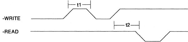
Figure 1-56. Write to Palette Address
Register
|
Symbol |
Write
to Register |
40
column and 320APA (ns) |
80
column and 640APA(ns) |
|
t1 |
Followed
by Write |
240 |
120 |
|
t2 |
Followed
by Read |
240 |
120 |
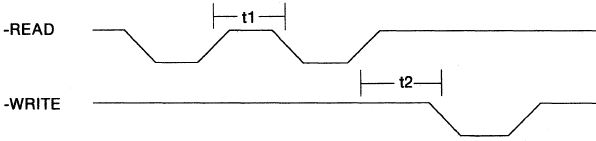
Figure 1-57. Read Palette Address
Register
|
Symbol |
Read
from Register |
40
column and 320 APA (ns) |
80
column and 640 APA (ns) |
|
t1 |
Followed
by Read |
240 |
120 |
|
t2 |
Followed
by Write |
240 |
120 |
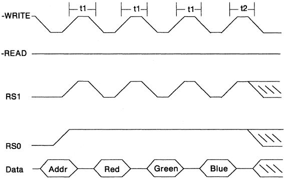
Figure 1-58. Write Color followed by a
Read
|
Symbol |
Write
to Register |
40
column and 320APA (ns) |
80
column and 640APA(ns) |
|
t1 |
Followed
by Write |
240 |
120 |
|
t2 |
Followed
by any Read |
240 |
120 |
Figure 1-59. Write Color followed by a
Write
|
Symbol |
Write
to Register |
40
column and 320APA (ns) |
80
column and 640APA(ns) |
|
t1 |
Followed
by Write Color |
240 |
120 |
|
t2 |
Followed
by any Read |
240 |
120 |
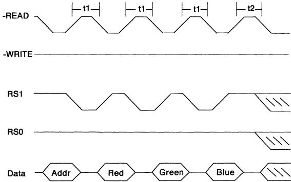
Figure 1-60. Read Color followed by a
Read
|
Symbol |
Read
Color |
40
column and 320APA (ns) |
80
column and 640APA(ns) |
|
t1 |
Followed
by Read Color |
240 |
120 |
|
t2 |
Followed
by any Read |
480 |
240 |
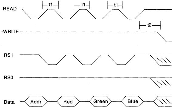
Figure 1-61. Read Color followed by a
Write
|
Symbol |
Read
Color |
40
column and 320APA (ns) |
80
column and 640APA(ns) |
|
t1 |
Followed
by Read Color |
240 |
120 |
|
t2 |
Followed
by any Write |
480 |
240 |
Connector [System Board]
The display connects to a 14-pin connector on the system board. The following are the pin numbering and signal assignments for the video connector.
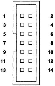
Figure 1-62. Display Connector
|
Pin
No. |
Signal
Name |
|
1 |
Ground
(Analog) |
|
2 |
Red
Video |
|
3 |
Ground
(Analog) |
|
4 |
Green
Video |
|
5 |
Ground
(Analog) |
|
6 |
Blue
Video |
|
7 |
Ground
(Analog) |
|
8 |
Ground
(Signal) |
|
9 |
Horizontal
Sync |
|
10 |
Ground
(Signal) |
|
11 |
Vertical
Sync |
|
12 |
Ground
(Signal) |
|
13 |
Monitor
Sense 0 |
|
14 |
Monitor
Sense 1 |