ALTERA
NOTE: We have modern
CPLDs and whatnot, so this programmer is sorta outdated, but
it supported MCMAP which could autogenerate an ADF. My
unlearned understanding: MCMAP generates the file, LogicMap
II actually programs the device. The LP5 / LP6 provides
power and control to the external PLE3-12. The PLE3-12 needs
a PLEJ2001 adapter to go from the DIP sockets on the PLE3-12
to the 84 pin EPB2001.NOTE: The PLE3-12 is compatible with the PLE3-12A. The -12A adds support for ALTERA MAX devices.
EPB2001 Micro Channel Interface 84-pin
EPB2002A DMA Arbitration Support 28-pin
1993 Altera Data Book [Bitsavers]
Application Note 95 In-System Programmability in MAX Devices [JTAG on LP6]
Missing ALTERA Publications:
Application Note 14 IBM PS/2 Add-On Card Interfacing
Application Note 15 IBM PS/2 Add-On Card Software Design
Micro Channel Adapter Handbook (April 1990) [misplaced my copy]
"Hands-On Experience Paves the Way for Future MCA Designs". EDN v34 #23, Nov 9, 1989 by Tom Darbonne.
Logic Programmer Cards LP5 / LP6 [ordering codes PLP5, PLP6]
These cards generate programming waveforms and voltages for the Master Programming Unit (MPU). The LP6 card is ISA, the LP5 card is MCA [PS/2 50, 60, 70, and 80 and compatible Micro Channel computers]. These cards are software-controlled and can be installed into any full-length expansion slot in a computer.
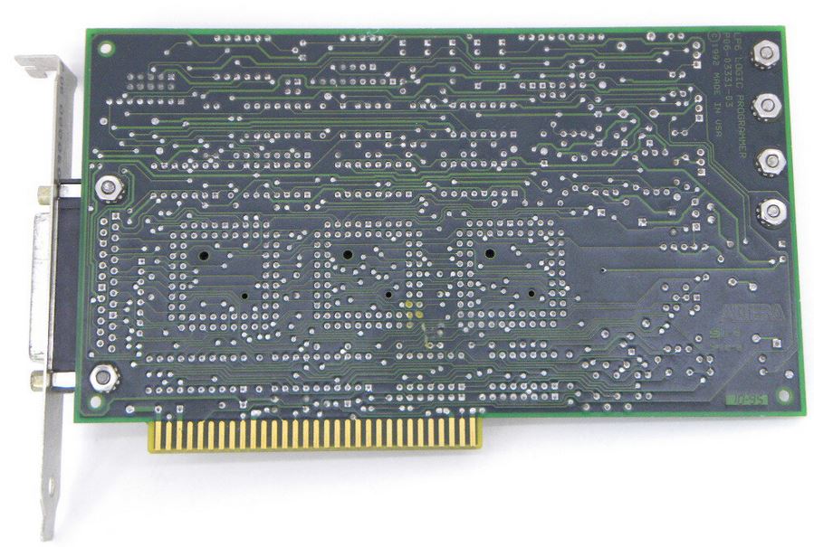
LP6 Front [Full size]

NOTES: I don't have any documentation on this card. My SWAG is the LP5 is similar.
D2,3,4,6,7 are LEDs, function UNK
U1,2,11 are voltage regulators? My SWAG is to set the programming voltages.
Q5 ? BiFET?
P1 appears to be a Bitblaster / Byteblaster 10-pin port? Dunno, we have the 25 pin port to talk to / power the PLE-12 [A] MPU. The PLE3-12A [pictured] can talk to later MAX devices, so this MIGHT be a JTAG.
P2 is a 25 pin port that connects to the PL-MPU [PLE3-12]. It is NOT a parallel port !
NOTE: Do NOT plug the PL-MPU ribbon cable into the system's parallel port ! I do not know if the PLE3-12 just won't work, or if any damage to either the system or PLE3-12 will occur... LFO
SW sets the I/O address for the card.
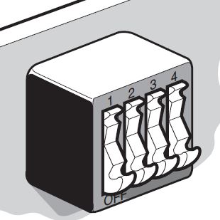
In this illustration, all switches are pushed in at the top [ 1 = ON / UP]
|
Base I/O |
SW Setting |
|||
|
[280 Default] |
1 |
2 |
3 |
4 |
|
270 |
0 |
0 |
0 |
0 |
|
260 |
1 |
0 |
0 |
0 |
|
250 |
0 |
1 |
0 |
0 |
|
240 |
1 |
1 |
0 |
0 |
|
230 |
0 |
0 |
1 |
1 |
|
220 |
1 |
0 |
1 |
0 |
|
210 |
0 |
1 |
1 |
0 |
|
200 |
1 |
1 |
1 |
0 |
|
2F0 |
0 |
0 |
0 |
1 |
|
2E0 |
1 |
0 |
0 |
1 |
|
2D0 |
0 |
1 |
0 |
1 |
|
2C0 |
1 |
1 |
0 |
1 |
|
2B0 |
0 |
0 |
1 |
1 |
|
2A0 |
1 |
0 |
1 |
1 |
|
290 |
0 |
1 |
1 |
1 |
|
280 |
1 |
1 |
1 |
1 |
1 = ON / UP
0 = OFF / DOWN
J1 is a four pin header, unknown.
1 2
B W
3 4
LP6 Back [Full Size]
Master Programming Unit PL-MPU
The MPU connects to a Logic Programmer card via a 25-pin ribbon cable. It receives power from the Logic Programmer card and does not require an external power supply. Programming and functional test information is transmitted from the Logic Programmer card through the ribbon cable to the MPU. A programming indicator LED on the MPU lights up when the unit is active.
When used with the appropriate adapter, the MPU automatically tests for continuity between the device leads and the programming socket before programming. It can also apply test vectors to functionally test and verify programmed Altera devices. Test vectors can be created in waveform or text format in the MAX+PLUS II Waveform Editor or Text Editor and applied to the device; results can be viewed in waveform or text format.
NOTE: Do NOT plug the PL-MPU ribbon cable into the system's parallel port ! I do not know if the PLE3-12 just won't work, or if any damage to either the system or PLE3-12 will occur... LFO