IBIN-PS/2
@6571.ADF IBIN-PS/2 Interface Card [IBM INterface or IBIN]
Interface for IBM PS/2 and Compatibles with MC Architecture 501-911-01B
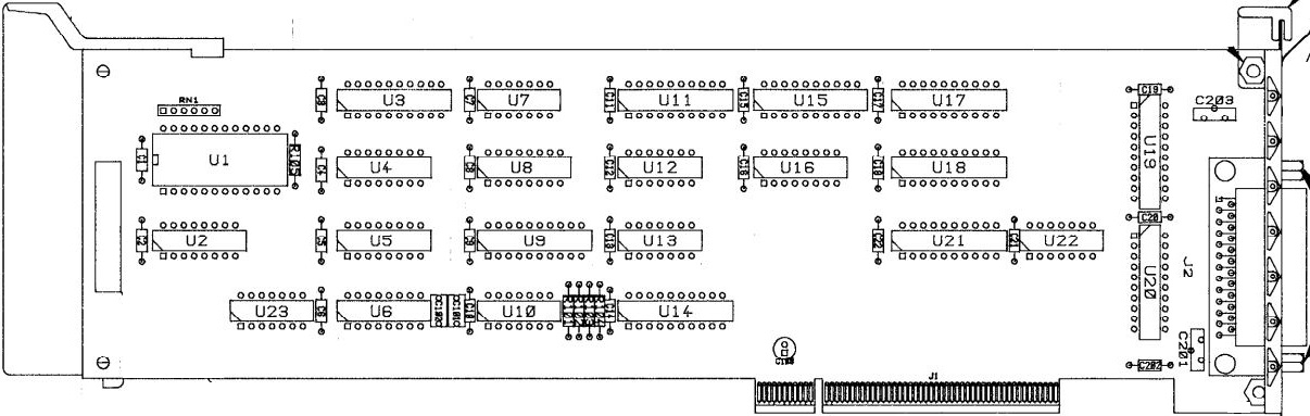
| J1
PS/2 Edge Connector J2 DB25 port U1 8254 U2 74LS367 U3 74LS240 U4 74LS175 U5 74LS138 U6 74LS139 U7 74LS74 U8,9,14 16L8 U10 74LS14 |
U11
74LS794 U12,13 74LS38 U15 74LS645 U16 74LS163 U17 74LS794 U18 74LS688 U19 74LS645 U20 74ALS533 U21 74LS373 U22 7400 U23 74LS00 |
J11 is the DB25 port on the 500/575 system board.
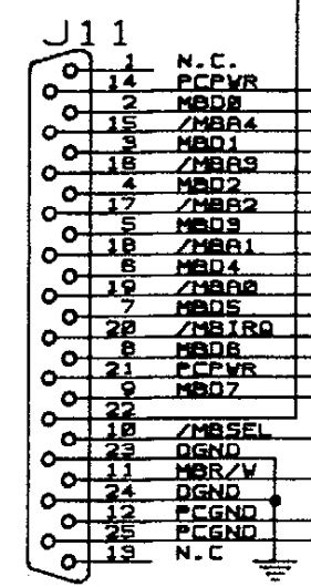
| 1
N.C 2 MBD0 3 MBD1 4 MBD2 5 MBD3 6 MBD4 7 MBD5 8 MBD6 9 MBD7 10 /MBSEL 11 MBR/W 12 PCGND 13 N.C. |
14
PCPWR 15 /MBA4 16 /MBA3 17 /MBA2 18 /MBA1 19 /MBA0 20 /MBIRQ 21 PCPWR 22 PCVCC 23 DGND 24 DGND 25 PCGND 0 |
Pins 14,21 are PCPWR. These pins supply power for the analog power supply in external devices. This power should be routed direct from the PS2 edge connector.
Pin 22 is PCVCC. This pin provides VCC power to the external devices. This power should be routed from the power grid on this ASSY [adapter, I assume]
PCVCC and PCPWR should be tied together at the PS2 edge connector only to reduce noise in the external equipment tied to J2.
GND on Pins 12,25 is PCGND, this GND should be run direct to the PS2 edge connector to minimize noise in chassis connected to J2.
GND on Pins 23,24 is DGND. This should run to the GND net of this circuit directly. DGND and PCGND should be tied together only at the PS2 edge connector.