PS/2 Type 3 DMA
Arbitrated Parallel Port
Folks, I've been bedeviled by the DMA Arbitrated parallel port [Type 3] since the late 90's. All the stuff on this page is my [failing?] attempt to understand the PS/2 Type 3 parallel port, from physical pin-out to registers. I do have a copy of "The Parallel Port Complete", but it seems to be utterly devoid of any discussion of interfacing a Type 3 port to an ECP port. YMWV, LFO.
NOTE: Some signals are active low, for example "-ACK". But another naming convention is "nACK", which IMHO has benefits, especially when naming images. LFO
US5239627A Bi-Directional Parallel Printer Interface
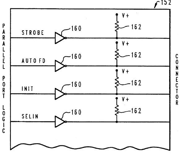
US5553306A - Method and apparatus for controlling parallel port drivers in a data processing system NOTE: Emulates Open Collector or Totem Pole circuit
| Open Collector Drivers |
Open Collector / Totem Pole Drivers |
 |
 |
| 160 - Invertor open collector 162 - Pullup resistor |
160 - S05 inverter 162 - pullup resistor 164 - LS125 three state logic 166 - resistor 168 - pullup resistor 170 - Output node 172 - AND logic gate 174 - Enable input 176 - Control line |
US5600793A - Method and system of bi-directional parallel port data transfer between data processing systems
US5299314A XIRCOM Pocket LAN Adapter
ibm_hitrc09-2 HITR - Common Interfaces, 1st Ed. (Oct 90) Parallel Port Controller
Interfacing Articles by Craig Peacock
Interfacing the Standard Parallel Port Compatible
Interfacing the Enhanced Parallel Port
Interfacing the Extended Capabilities Port Extended
Understanding the New Developments in Parallel Ports by Douglas Boling
Parallel Port Information System v 1.45, Jay Lowe, Don Schuman 27 Oct 1994
IEEE 1284 – Updating the PC Parallel Port NI - AN 062
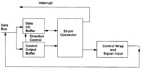
Parallel Port Block Diagram
Parallel Port Connector Pinout [Type 3]
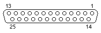
| Pin | Signal Name | Pin | Signal Name |
|---|---|---|---|
| 1 | -STROBE | 14 | -AUTO FD XT |
| 2 | Data 0 | 15 | -ERROR |
| 3 | Data 1 | 16 | -INIT |
| 4 | Data 2 | 17 | -SLCT IN |
| 5 | Data 3 | 18 | Ground |
| 6 | Data 4 | 19 | Ground |
| 7 | Data 5 | 20 | Ground |
| 8 | Data 6 | 21 | Ground |
| 9 | Data 7 | 22 | Ground |
| 10 | -ACK | 23 | Ground |
| 11 | BUSY | 24 | Ground |
| 12 | PE | 25 | Ground |
| 13 | SLCT | ||
SPP, DMA, and ECP Pinouts
| Pin |
SPP |
DMA |
ECP |
Funct |
| 1 |
nStrobe |
-STROBE |
HostCLK |
|
| 2-9 |
Data 0-7 |
Data 0-7 |
Data 0-7 |
|
| 10 |
nACK |
-ACK |
PeriphCLK |
|
| 11 |
BUSY |
BUSY |
PeriphACK |
|
| 12 |
PE |
PE |
nAckReverse |
|
| 13 |
SELCT |
SLCT |
X-Flag |
|
| 14 |
nAuto Linefeed |
-AUTO FD XT |
HostAck |
|
| 15 |
nERROR |
-ERROR |
PeriphReq |
|
| 16 |
nINIT |
-INIT |
nReverseReq |
|
| 17 |
nSELPRINT |
-SLCT IN |
1284Active |
|
| 18-25 |
Ground |
Ground |
Ground |
NOTE: A leading "n" or "-" both mean the signal is active low.
Address Selection
| Port | Parallel Data Register | Device Status Register | Device Control Register | Interface Control Register | Interface Status Register | Reserved Register | IRQ |
| SPP | 0378 | 0379 | 037A | NA | NA |
037B | 7 |
| DMA | 0378 | 0379 | 037A | 037B | 037C | 037D | 7 |
NOTE: DMA Arbitrated port "Parallel 2" aligns with the clone "LPT1".
Extended Mode
The extended mode option is selected through the POS function during system board setup. The extended mode makes the parallel port an 8-bit parallel bidirectional interface and makes DMA available for Type 2 and Type 3 controllers. The parallel port provides half duplex transfers when in bidirectional operation mode. Direction is determined by bit 5 of the Device Control register and DMA is controlled through the Interface Control register.
Arbitration Level (Type 2 and Type 3)
The Type 2 controller is fixed at arbitration level 6 and cannot be set through POS. The Type 3 controller allows arbitration levels to be configured to any level through the POS function.
Parallel Port Controller Programming Considerations
The interface has three registers that respond to input and output instructions. The three registers are:
A read and write Parallel Data register
A read only Device Status register
A read and write Device Control register.
Type 2 and Type 3 controllers have three additional registers:
A read and write Interface Control register
A read only Interface Status register
A write only Reserved register.
These registers are available in extended mode only.
During POST the parallel port is configured as an output port. POST status information is written to this port during the power-on initialization or the initialization caused by a reset from the keyboard (Ctri + Alt + Del).
DMA Mode (Type 2 and Type 3 Only)
Single DMA transfers are supported both when sending and receiving. The DMA enable bit in the Interface Control register is set to 1 when DMA service is requested.
The parallel port has two idle states while it is in the DMA mode:
Not ready (end-of-data bit = 1): Any request generates an interrupt if the interrupt is enabled. This state is entered after completing a DMA transfer or after setting the End of Data bit (bit 6) in the Interface Control register to 1.
Ready (end-of-data bit = 0): While in this state, a pulse on the ‘-acknowledge’ signal starts a DMA transfer. This state is entered after the Start DMA bit or the Reset End of Data bit (bit 6) is set in the Interface Control register to 1.
in addition, there are two data transfer states:
Send byte: This state is entered when bit 5 of the Device Control register is set to 0 and a Start DMA or an ‘-acknowledge’ signal is set. A DMA fetch transfer is initiated, the data is placed on the interface, and the ‘strobe’ signal line is pulsed.
Receive byte: This state is entered when the direction bit is set to 1 and an ‘-acknowledge’ signal is set. A DMA store is initiated and the ‘strobe’ signal is pulsed to acknowledge the completion of the operation. The incoming data is latched at the trailing edge of the ‘-acknowledge’ signal.
Sending
Writing a 1 to the start-DMA bit in the Interface Control register initiates the DMA transfer to the attached device. (The enable DMA bit must have been set to 1 in a previous operation). The DMA Controller channel and the direction of the transfer are set before
writing a 1 to the start-DMA bit. If the device is not busy, the parallel port controller requests the system bus. After control of the bus is gained, the following sequence of events occur:
1. Data is read from memory and written to Parallel Data register by DMA controller.
2. Data is carried to attached device using ‘strobe’ signal on the parallel interface.
3. The ‘strobe’ signal is activated automatically after the Parallel Data register is written.
4. The device issues the ‘-acknowledge’ signal when the data transmission is completed.
NOTE: The ‘-acknowledge ’ signal is used to trigger the next DMA transfer, if the end-of-data latch (bit 6 of the Interface Status register equals 0) is reset and DMA is enabled. In addition, the attached device must hold the ‘busy’ signal inactive for the parallel port to
issue a DMA request.
When a terminal count is reached during a DMA transfer, the end-of-data latch is set and the next DMA transfer is prevented. It is known that the DMA controller has transferred the last byte of data to the parallel port controller. However, it is not known if the attached device has received the last byte of data. The parallel port controller is designed to interrupt at the ‘-acknowledge’ signal after the end-of-data latch is set. At the completion of a DMA transfer, the parallel port controller will interrupt if the terminal-count interrupt-enable bit is set.
By setting the end-of-data (EOD) bit in the Interface Control register, the current DMA operation will be terminated. It should be noted that no interrupt will be generated by setting this bit.
This causes an effect similar to terminal count. One additional byte of data may be sent depending on the timing of the setting of the bit.
Disabling the DMA while a DMA transfer is in progress stops the generation of ‘strobe’ signals and causes an interrupt to end the DMA transfer.
Receiving
The DMA channel must be initialized prior to receiving data from the attached device. When the parallel port controller is ready to receive data from the attached device, the parallel port controller uses the ‘-acknowledge’ signal. The ‘-acknowledge’ signal initiates the DMA transfer to the system memory, if the end-of-data latch is reset and DMA is enabled. Data transmission allows the parallel port controller to request the system bus. After control of the bus is gained, the following sequence of events occur:
1. Data in Parallel Data register of parallel port controller is read and then written to memory by the DMA controller.
2. The ‘strobe’ signal is activated after the read command pulse to the Parallel Data register.
The parallel port controller cannot receive subsequent data until the previous data has been read by the DMA controller and transferred to the system memory. When the ‘-acknowledge’ signal goes low, (data is being placed on the bus) the parallel port controller asserts the ‘-autofeed’ signal (-AUTOFD) line high to inform the attached device of a busy state. After the DMA controller reads the data from the Parallel Data register, a ‘strobe’ signal is generated automatically as an acknowledgement of data transmission. A positive edge of the ‘strobe’ signal resets the -AUTOFD line !fow to tell the attached device that the controller is not busy. The ‘busy’ signal has no effect in
receive mode.
To determine the end of a DMA transfer, the parallel port controller interrupts if the terminal-count interrupt-enable bit is on. When the terminal count is reached during a DMA transfer, the end-of-data | latch is set to prevent the next DMA cycle and an interrupt occurs. The DMA controller has transferred the last byte of data to the memory.
Interrupt Condition
When enabled, the following event can cause an interrupt:
Any transition of the ‘-error’ signal
Any transition of the ‘paper end’ signal
Any transition of the ‘select’ signal
The positive edge of the ‘-acknowledge’ signal
— When DMA is disabled
— When DMA is enabled and end-of-data is set
Terminal count while DMA is enabled while receiving.
Output Data Rate
The approximate time between two data bytes in a DMA operation is 5 microseconds, assuming that the attached device returns the ‘-acknowledge’ signal to the ‘strobe’ signal immediately. tn addition, the ‘-acknowledge’ signal is 1.0 microseconds wide (the ‘-acknowledge’ signal falls low and not later than approximately 1.0 microseconds after the rising edge of the ‘-strobe’ line). To calculate the data rate, the delay from the ‘-strobe’ signal to the ‘-acknowledge’ signal on the attached device side should be added for each transmission. The transfer rate varies according to the DMA channel usage of the system.
Register Definitions Pages 11-18 ibm_hitrc09-2 HITR - Common Interfaces
The following definitions apply to all types of parallel port controllers, unless specified otherwise. All reserved bits will be written as 0, and read as a 1.
Parallel Data Register
The Parallel Data register is a read and write register. Its output drivers are enabled by the direction bit in the Device Control register. A read operation returns the output data, if the output drivers are enabled or if data is read from the attached device when the drivers are not enabled. Care must be taken not to enable the drivers when the attached device is also driving the interface.
CAUTION:
Damage to the system can occur if the controller and the attached device are driving data onto the data lines at the same time. Therefore, do not enable the drivers when the attached device is driving the Interface.
Parallel Data register is an 8-bit data register for both the compatible and extended modes. In compatible mode, writing to this register immediately presents data to the connector. Reading this register returns the last byte written.
In extended mode, writing to this register latches the data; however, the data is presented to the connector only if the direction bit is 0 (write). Reading the register returns either:
- The last byte written, if the direction bit is 0
- The data on the connector from the attached device, if the direction bit is 1.
Device Status Register
Read-only register contains the status of attached device and status of the interrupt.
| Pin | Bit | Name | Function |
| 11 | 7 | -BUSY | When set to 0, printer is busy and can't accept data. |
| 10 | 6 | -ACKNOWLEDGE [-ACK] | When bit is pulsed, the device has received a character and is ready to accept another. |
| 12 | 5 |
PAPER END [PE] | When set to 1, printer has detected end of the paper. |
| 13 | 4 | SELECT [SLCT] |
When set to 1, the printer has been selected. |
| 15 | 3 | -ERROR | When set to 0, printer has encountered an error condition. |
| ? | 2 | -IRQ STATUS | Set to 0 - device has acknowledged previous
transfer using the ‘-acknowledge’ signal. Set to 1 - Device Status register or interface Status register is read. An interrupt is pending when set to 0. NOTE Used in non-DMA mode only. |
| NA | 1,0 | Reserved | These bits are reserved. |
Device Control Register [Type 3]
This is a read and write register that controls lines to the attached device. Reading this register returns the last byte written to the register, if the line is not driven by the attached device. The direction bit can be updated at any time, but the effect of the bit is masked when in non-extended mode (in compatible mode the direction is always out, even if the bit reads as 1).
This is for Type 3 NOT for Types 1 and 2!
| Pin | Bit | Name | Function |
| ? | 7 | Autostrobe | Set to 1 enables ‘Autostrobe’ signal. |
| NA | 6 | Reserved | Must be set to 1. A read operation returns a value of 1. |
| ? | 5 | Direction | Direction of data register. Set to 0, data drivers enabled, parallel data placed on output data lines. A read operation returns 1 in non-extended mode and last value written in extended mode. |
| ? | 4 | IRQ Enable | Enables parallel port interrupt. When 1, interrupt
occurs when ‘-acknowledge’ signal changes from
active to inactive (NOTE non-DMA mode only). |
| 17 | 3 | SLCT IN | ‘select in’ signal. When set to 1, printer is selected. |
| 16 | 2 | -INIT | ‘initialize’ signal. When set to 0, printer is initialized. |
| 14 | 1 | AUTO FD XT | ‘automatic feed XT’ signal. When set to 1, printer automatically spaces paper up one line for every carriage return. |
| 1 | 0 | -STROBE | ‘strobe’ signal to printer. When set to 1, data is clocked to printer. |
CAUTION: Do not enable the drivers for the data lines while the attached device is driving them.
Interface Control Register [Types 2 and 3]
This register controls the various functions available in the interface. All bits read as 1 in non-extended mode. Bits 1, 6, and 7 always read as 1.
| 7 | Start DMA | Writing a 1 initiates DMA transfer. Enable DMA (bit 0) must have been set to 1 in a previous write operation, otherwise results are indeterminate. Reading this bit always returns as a 1. |
| 6 | Reset EOD | Setting this bit to 1 resets end-of-data latch, which allows port to honor DMA transfer requests by ‘-acknowledge’ signal. Reading this bit always returns a 1. |
| 5 | Enable TC/ACK Interrupt | Setting this bit to 1 enables interrupts to occur
whenever terminal count is achieved, or whenever an
‘-acknowledge’ signal occurs with end-of-data latch
set. A 0 clears the terminal count ‘-acknowledge’ signal in Interface Status register and removes any pending interrupts caused by terminal count. NOTE This bit is used only in DMA mode. |
| 4 | SLCT IRQ Enable | bit is valid in extended mode and setting to 1 enables interrupts to occur on either edge of SELECT. Resetting this clears ‘select interrupt request’ signal (SLCT IRQ) in Interface Status register. |
| 3 | -ERROR IRQ Enable | valid in extended mode and enables interrupts to occur on either edge of an ‘-error’ signal. Resetting this clears ‘error interrupt request’ signal (-ERROR IRQ) in the Interface Status register. |
| 2 | PE IRQ Enable | valid in extended mode and enables interrupts to occur on either edge of a ‘paper end’ signal. Resetting this clears ‘paper end interrupt request’ (PE IRQ) in the Interface Status register. |
| 1 | Set EOD | Setting this bit to 1 sets end-of-data latch which stops DMA transfers before terminal count is reached. Reading this bit always returns a 1. This output generates a pulse and always reads as 1. |
| 0 | Enable DMA | enables DMA function. Whenever this is set from reset condition, the end-of-data latch (bit 1) must also be set to prevent unknown states. The extended mode must be set in the POS register before this bit can be set. |
NOTE: Writing certain bit combinations of the Interface Control register may cause unexpected results. Those bit combinations listed as reserved in the following figure must not be used.
Interface Control Register DMA Functions
| Bits 7,6 | Bits 1,0 | Function |
| 00 | 00 | Reserved |
| 00 | 01 | No Change to DMA Operation |
| 00 | 10 | Disable DMA |
| 00 | 11 | Halt DMA or Enable DMA |
| 01 |
00 | Reserved |
| 01 | 01 | Set Ready-to-Start DMA in Receive Mode |
| 01 | 10 | Reserved |
| 01 | 11 | Reserved |
| 10 | 00 | Reserved |
| 10 | 01 | Start DMA in Send Mode |
| 10 | 10 | Reserved |
| 10 | 11 | Reserved |
| 11 | 00 | Reserved |
| 11 | 01 | Reserved |
| 11 | 10 | Reserved |
| 11 | 11 | Reserved |
Interface Status Register
This is a read-only register and is used to convey the status of the parallel interface. Reading this register resets the interrupt pending status bits and resets the interrupt request. The interrupt handler must save the status or process it completely before returning.
Disabling the interrupts with the Interface Control register also clears the corresponding interrupt-request bit. All bits in this register read as 1 in compatible mode.
NOTE: Because reading the register resets the interrupt status (bits 2 through 5), there is a small window where the interrupting condition, if it occurs at the end of the read operation, will not set the corresponding interrupt status bit (the interrupt is also prevented). A periodic check of the corresponding status bits in the Device Status register and the EOD bit in this register can be used to detect this condition.
Interface Status Register (Type 2 and Type 3)
| Bit | Name | Function |
| 7 | Reserved | This bit is reserved. |
| 6 | EOD | When EOD bit is 1, the end-of-data latch is set and the parallel port is not ready to perform a DMA transfer. This occurs when the terminal count is reached or when the latch is set through the set-end-of-data-latch bit in the Interface Control register. |
| 5 | TC/ACK Interrupt | When the TC/ACK interrupt bit is set to 1, the pending interrupt is caused by the terminal count or by an '-acknowledge’ signal. If the EOD bit is 1, the interrupt was caused by the terminal count, otherwise it is caused by the ‘acknowledge’ signal. |
| 4 | SLCT Interrupt | When the SLCT interrupt bit is 1, the pending interrupt is caused by any transition of the ‘select’ signal. |
| 3 | Error Interrupt | When error interrupt bit is 1, the pending interrupt is caused by any transition of the ‘error’ signal. |
| 2 | PE Interrupt | When the PE interrupt bit is set to 1, the pending interrupt is caused by any transition of the ‘paper end’ signal. |
| 1,0 | Reserved | These bits are reserved. |
Reserved Register Initialization
NOTE: This register must be loaded with a value of Hex 16 before using DMA mode.
NOTE: Reading this register gives unpredictable values.
Parallel Port Timing
Timing for the parallel port depends on the devices connected to it. Minimum requirements for parallel-port signal timing and any device that may be attached to the parallel port are:
Parallel-Port Timing Sequence
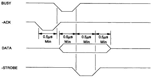
The DMA (Types 2 and 3) and Autostrobe (Type 3) functions will generate these timings automatically. In sending modes, -STROBE will be activated 1.0 ±0.25 microseconds after the data is placed on the output data lines. The -STROBE pulse width is 1.0 ±0.25
microseconds. In DMA receive mode, a strobe pulse 1.0 ±0.25 microseconds wide will be generated as soon as the data has been read from the data lines.
For specific signal timing parameters, refer to the specifications for the equipment connected to the parallel port connector.
Signal Descriptions
Receiver A Specifications
High-Level input Voltage 2V Minimum
Low-Level Input Voltage 0.8V Maximum
High-Level Input Current 40 WA Maximum
Low-Level Input Current -0.8 mA Maximum
Driver B Specifications
Sink Current 24 mA Maximum
Source Current -2.6mA Maximum
High-Level Output Voltage 2.4 Vdc Minimum
Low-Level Output Voitage 0.5 Vde Maximum
Driver C Specifications
Sink Current 20 mA Maximum
Source Current Open Collector
High-Level Output Voltage Open Collector
Low-Level Output Voltage 0.5 Vdc Maximum
Data Lines [D0-D7] (Pins 2-9)
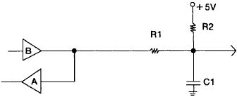
R1 33 Ohms
R 2 2 kilo ohms or Not Present
C1 0.0022 µF or Not Present
Receiver A
Driver B
-STROBE (Pin 1)
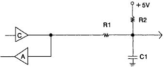
R1 33 ohms
R2 2 kilo ohms to 4.7 kilo ohms
C1 0.0022 µF or Not Present
Receiver A
Driver C
-AUTOFDXT, -INIT, -SLCTIN (Pins 14, 16, 17)
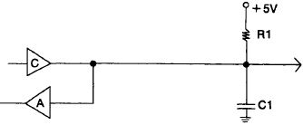
R1 2 kilo ohms to 4.7 kilo ohms
C1 0.0022 µF or Not Present
Receiver A
Driver C
-ACK, BUSY, PE, SLCT, -ERROR (Pins 10, 11, 12, 13, 15)
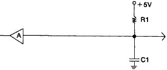
R1 1 kilo ohms to 10 kilo ohms or Not Present
C1 0.00068 to .0022 µF or Not Present
Receiver A
XT, AT, and PS/2 Parallel Ports [from US5299314A XIRCOM patent]
| XT |
AT |
PS/2 |
 |
 |
 |
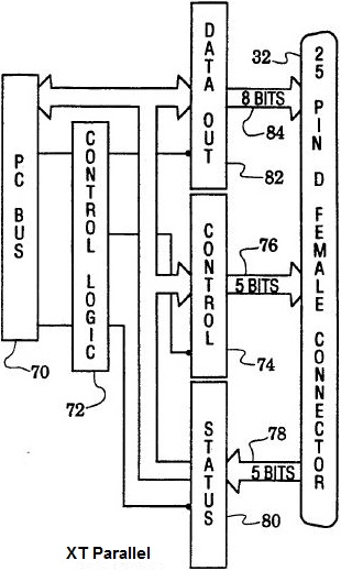
XT parallel port control logic is configured to provide eight unidirectional-out data lines, five unidirectional-out control lines and five unidirectional-in status lines. In the XT configuration, the unidirectional data lines emanate from a unidirectional-out data latch and are intended to be used solely for writing to a peripheral device and not for reading
therefrom.
In the standard IBM XT configuration, the PC bus 70 is internally connected through control logic 72 to a set of control latches 74. Five bit lines 76 connect the unidirectional out control latches 74 to pins on the connector 32. Five additional pins on the connector 32 connect via five status lines 78 to unidirectional in status latches 80 and then to the
control logic 72. Most significantly, note that a set of eight unidirectional out data latches 82 connect the bus 70 through lines 84 to pins on the connector 32. The data latches 82 are unidirectional out to connector 32 and do not allow for reading data from the connector 32 back into the PC bus 70 via the data lines 84. As will be seen hereinafter, in accordance with the present invention, the five status lines 78 are used by the network adapter 10 for reading data in to the PC bus 70, four bits at a time. This data transfer mode will hereinafter sometimes be referred to as a double quasi nibble
transfer mode.
The AT configuration differs from the XT primarily in that it additionally has an in data latch for reading data from the data lines.
The IBM AT parallel port configuration differs from the XT configuration in that it includes eight data out-latches 88 and eight data in-latches 90 both connected to the eight data lines 92. The AT parallel port was designed only with data output capability in mind with a readback capability, i.e. via data in-latches 90, for detecting faults. The data out-latches 88 are not tristatable, i.e. they are always driving out. In operating with the AT configuration, the network adapter 10 is able to force the data out latch 88 to all ones and is able to read data in, eight bits in parallel, via the data in-latch 90, because of its TTL implementation which allows a TTL ground to over come a TTL high level. In summary, when properly driven, the AT parallel port inherently allows data bytes to move bidirectionally without any control of the bidirectionality.
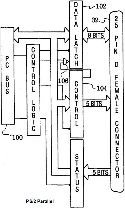
The PS/2 configuration differs further in that it includes a bidirectional data latch which is set to either read data in or write data out dependent upon the state of a control bit.
In the PS/2 parallel port configuration, the PC bus 100 is connected through a bidirectional data latch 102 to the parallel port connector 32. In this configuration, a bit within the control latch 104 controls the directionality of the data latch 102 via gate
106. A network adapter 10 in accordance with the present invention sets the bit in the control latch 104 to set the directionality of the data latch 102, that is to either transfer data into or out of the data latch 102 with respect to the connector 32.
Summary
Thus, in summary, a standard XT parallel port is strictly unidirectional, standard AT parallel port was designed to be unidirectional but as a consequence of it being able to detect faults, can be used in a bidirectional fashion, and a standard PS/2 parallel
port, is truly bidirectional and its directionality is controlled by a control bit.
DMA Mode PS/2 Connections
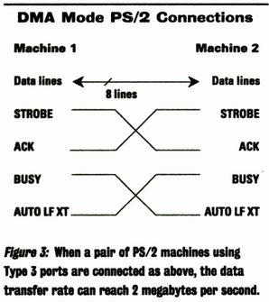
NOTE: "AUTO LF XT" does not exist on a Type 3 port. Such a term comes from the Intel 386SL chip, used on laptops. "AUTO LF XT" is redefined as "Data Strobe" under the 386SL's "Fast Mode". Should this be "AUTO FD XT" instead ???
If two PS/2s are to transfer data using the DMA mode, their two parallel ports should be connected in the manner shown in Figure 3. This particular configuration allows the two parallel-port controllers to produce the proper handshaking for the DMA transfer.
So connected, a pair of PS/2s using their DMA parallel ports can transfer data at up to 2MB per second, a transfer rate rivaling that of some hard disk controllers. And this speed is available with almost no work from the processor.
The DMA mode was not the only improvement made in the Type 3 port. The port also has expanded interrupt capabilities. The parallel-port controller can interrupt the processor on changes in the ERROR, PAPER END (PE), and SLCT. Like all previous parallel ports, the new port can also interrupt the processor when the ACK line is lowered.
Three new registers were added to the parallel-port register set to control the enhanced Type 2 and Type 3 parallel ports. This presented a problem when the port was configured at the old standard starting I/O address of 3BCh, because if the new registers were placed at their logical location (Just after the other port registers) they would overlap the registers that control the VGA palette. To solve this problem, the Type 3 parallel port can be addressed at two different I/O address ranges if configured as parallel port 1. When the parallel port is configured as LPT 2, 3, or 4, the dual addressing is not necessary.