Bus Interface Unit
(BIU)
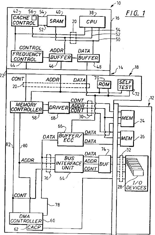
The CPU portion operates at 50 MHz and the base portion operates at 40 MHz
Further study is required, but I -think- IBM figured there was too many problems with a 20MHz clocked complex and system I/O [on MCA] so they had to translate and buffer in order to synchronize between the complex and the MCA.
T1 - 10MHz to MCA
T2 - 25MHz to MCA
T3 - 20MHz to MCA
T4 - 20MHz to MCA
Also, the creation of an ASIC to translate between the system bus and I/O bus probably turned out to be quite useful.
System devices and I/O devices in dual bus architecture computer systems often communicate with each other at different rates and over different data transfer bandwidths. For example, whereas system devices may communicate over the system bus at a 32-bit data bus width, I/O devices may communicate over the I/O bus at 8-bit, 16-bit, or 32-bit data bus widths. Hence, overall system performance suffers when a system device, in control of both the system and I/O buses, either reads from or writes to a slower I/O device. This is compounded by 16-bit transactions to 8-bit I/O slaves and 32-bit transactions to 16-bit and 8-bit I/O slaves. In the case of write cycles, a system device must retain control of the system bus, for a time greater than that necessary to write data over the system bus, while the data is being written to the slower I/O device. In the case of read cycles, the slower I/O device cannot provide data to the system device over the I/O bus as fast as it can be read from the I/O device by the system device. It is an object of the present invention, then, to provide a bus interface unit in a dual bus architecture computer system which provides the translation logic required for synchronizing operation of the system bus and the I/O bus to compensate for devices which communicate to each other at different rates and over different data transfer bandwidths.
Figure 2 Block diagram of Bus Interface Unit
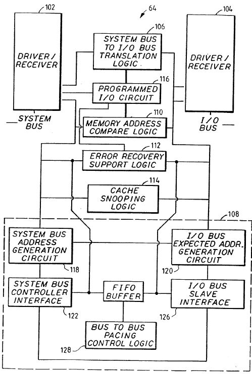
Referring to Figure 2, a schematic block diagram of the bus interface unit 64 of the system of Figure 1 is shown. Bus interface unit 64 provides the basis for implementation of the present invention by providing a bi-directional high speed interface between system bus 76 and I/O bus 32.
Bus interface unit 64 includes system bus driver/receiver circuit 102, I/O bus driver/receiver circuit 104 and control logic circuits electrically connected therebetween. Driver/receiver circuit 102 includes steering logic which directs signals received from the system bus 76 to the appropriate bus interface unit control logic circuit and receives signals from the bus interface unit control logic circuits and directs the signals to the system bus 76. I/O bus driver/receiver circuit 104 includes steering logic which directs signals received from the I/O bus 32 to the appropriate bus so interface unit control logic circuit and receives signals from the bus interface unit control logic circuits and directs the signals to the I/O bus 32.
The bus interface unit control logic circuits include system bus to I/O bus translation logic 106, I/O bus to system bus translation logic 108, memory address compare logic 110, error recovery support logic 112, and cache snooping logic 114. Programmed I/O circuit 116 is also electrically coupled to system driver/receiver circuit 102.
System bus to I/O bus translation logic 106 provides the means required for the DMA controller 60 or the memory controller 58 (on behalf of CPU 38) to act as a system bus controller to access the I/O bus 32 and thereby communicate with I/O devices 28 acting as slave devices on the I/O bus. Translation logic 106 translates the control, address and data lines of the system bus 76 into similar lines on the I/O bus 32. Most control signals and all address signals flow from the system bus 76 to the I/O bus 32 while data information flow is bi-directional. The logic which acts as system bus slave monitors the system bus 76 and detects cycles which are intended for the I/O bus 32. Upon detection of such a cycle, the system bus slave translates the timing of signals on the system bus to I/O bus timing, initiates the cycle on the I/O bus 32, waits for the cycle to be completed, and terminates the cycle on the system bus 76.
I/O bus to system bus translation logic 108 comprises system bus address generation circuit 118, I/O bus expected address generation circuit 120, system bus controller interface 122, FIFO buffer 124, I/O bus slave interface 126 and bus to bus pacing control logic 128. System bus controller interface 122 supports a high performance 32 bit (4 byte) i486 burst protocol operating at 40 MHZ. Data transfers of four, eight and sixteen bytes in burst mode and one to four bytes in no-burst mode are provided. I/O bus slave interface 126 monitors the I/O bus 32 for operations destined for slave devices on the system bus 76 and ignores those operations destined for the I/O bus 32. All cycles picked up by the I/O bus slave interface 126 are passed on to the FIFO buffer 124 and the system bus controller interface 122.
I/O bus to system bus translation logic 108 provides the means required for an I/O device 28 to act as an I/O bus controller to access system bus 76 and thereby read or write to system memories 24 and 26. In either of these operations, an I/O device controls the I/O bus. The asynchronous I/O bus interface 126, operating at the speed of the I/O device, permits the bus interface unit 64 to act as a slave to the I/O device controller on the I/O bus 32 to decode the memory address and determine that the read or write cycle is destined for system memories 24 or 26. Simultaneously, the system bus controller interface 122 permits the bus interface unit 64 to act as a controller on the system bus 74. The memory controller 58 (Figure 2) acts as a slave to the bus interface unit 64, and either provides the interface 64 with data read from system memory or writes data to system memory. The reads and writes to system memory are accomplished through the FIFO buffer 124, a block diagram of which is illustrated in Figure 3
Figure 3 Block diagram of BIU FIFO buffer
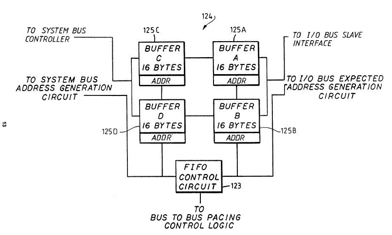
As shown in Figure 3, FIFO buffer 124 is a dual ported, asynchronous, bi-directional storage unit which provides temporary storage of data information between the system and I/O buses 76, 32. FIFO buffer 124 comprises four sixteen-byte buffers 125A- 125D and FIFO control circuit 123. The four buffers 125A-125D buffer data to and from I/O bus controllers and system bus slaves, thereby allowing simultaneous operation of the I/O bus 32 and the system bus 76. The FIFO buffer 124 is physically organized as two thirty-two byte buffers (125A/125B and 125C/125D). The system bus controller interface 122 and the I/O bus slave interface 126 each control one thirty-two byte buffer while the other thirty-two byte buffer operates transparent to them. Both of the thirty-two byte buffers are utilized for read and write operations.
Each FIFO 124A, 125B, 125C, 125D has an address register section either physically associated with the respective FIFO, or logically associated therewith. As data is transferred from the I/O bus 32 to FIFO 125A, the data will be accumulated until the 16 byte buffer is filled with 16 bytes of data, provided that the addresses are contiguous. If a non-contiguous address is detected by the address action, the FIFO 125A will transfer the stored data to FIFO 125C, and at the same time FIFO 125B will start to receive this data from the new non-contiguous address. FIFO 125B will continue just as FIFO 125A did until it is filled with 16 bytes of data, or another non-contiguous address is detected. FIFO 125B will then transfer the stored data to FIFO 125D, and FIFO 125A again starts to store data; thus, it is possible to store up to four 16 byte blocks of non-contiguous address data.
Further, by having two 32 byte buffers in parallel the reading and writing of data can be toggled between them thus giving an essentially continuous read or write function.
Moreover, by splitting the 32 byte buffers into two 16 bytes buffer sections which are coupled to other I/O bus 32 or system bus 26, the number of storage buffers can be increased with minimal impact on the performance of the FIFO as related to the capacitive loading on signals clocking data in or out of the storage registers. This is accomplished because for every two buffers added (in parallel) only half the capacitive loading is added to the loading of clock signals on each bus.
Additionally, by having two 16 byte buffers in series in each leg, once one of the 16 byte buffers is filled with data, such as in a read operation, the data can be transferred to the other 16 byte buffers in series so therewith, while the other parallel leg is accumulating data. Hence, there is no time lost in either accumulating data, or transferring the data from one bus to the other.
The logic for controlling the operation of the FIFO 124 is supplied by FIFO Control Circuit 123.
A particular I/O device 28 may write to system memories 24 or 26 via I/O bus in bandwidths of either 1, 2 or 4 bytes (i.e., 8, 16 or 32 bits). During writes to system memory by an I/O device 28, the first transfer of write data is initially stored in the FIFO buffer 125A or 125B. The I/O bus expected address generation circuit 120 calculates the next expected, or contiguous, address. The next contiguous address is checked against the subsequent I/O address to verify if the subsequent transfers are contiguous or not. If contiguous, the second byte or bytes of write data is sent to the same FIFO buffer 125Aor 125B. The FIFO receives data at asynchronous speeds of up to 40 megabytes per second from the I/O bus 32.
This process continues until either buffer 125A or 125B is full with a 16-byte packet of information or a non-contiguous address is detected. On the next clock cycle, assuming that buffer 125A is full, the data in buffer 125A is transferred to buffer 125C. Similarly, when buffer 125B is full, all of its contents are transferred to buffer 125D in a single clock cycle. The data stored in the buffers 125C and 125D is then written to system memory via an i486 burst transfer at the system bus operational speed. The operation of FIFO buffer 124 during a write to system memory by an I/O device is thus continuous, alternating between buffers 125A and 125B, with each emptying into adjacent buffer 125C or 125D, respectively, while the other is receiving data to be written to system memory. The FIFO buffer 124, then, optimizes the speed of data writes to system memory by (i) anticipating the ad- dress of the next likely byte of data to be written into memory and (ii) accommodating the maximum speed of write data from the FIFO buffer to system memory via the system bus 76.
During reads of data from system memory to an I/O device 28, FIFO buffer 124 operates differently. The system bus address generation circuit 118 uses the initial read address to generate subsequent read addresses of read data and accumulate data in buffer 125C or 125D. Because the system bus supports transfers in bandwidths of 16 bytes wide, the system bus controller interface 122 may prefetch 16-byte packets of contiguous data and store it in buffers 125C or 125D without the I/O bus 32 actually providing subsequent addresses, thus reducing latency between transfers. When buffer 125C is full of prefetched data, it transfers its contents to buffer 125A in one clock cycle. Buffer 125D similarly empties into buffer 125B when full. The data in buffers 125A and 125B may then be read by a particular I/O device controller in bandwidths of 1, 2 or 4 bytes. In this way, system bus address generation circuit 118 functions as an increment counter until instructed to by the I/O controller device to stop prefetching data.
Bus to bus pacing control logic 128 creates a faster access to system memory for high speed I/O devices. The bus to bus pacing control logic 128 overrides the normal memory controller arbitration scheme of system 10 by allowing an I/O device in control of the I/O bus 32 uninterrupted access to system memory during transfers of data by faster devices which require multiple cycles, rather than alternating access to the memory controller 58 between the I/O device and the CPU. Thus, even if a local device such as the CPU has a pending request for control of the memory bus during a multiple cycle transmission by an I/O device, the bus to bus pacing control logic 128 will grant the I/O device continued control of the memory bus.
Programmed I/O circuit 116 is the portion of the bus interface unit 64 which contains all of the registers which are programmable within the bus interface unit 64. The registers have bits associated therewith to determine whether a particular register is active or inactive. These registers define, inter alia, the system memory and expansion memory address ranges to which the bus interface unit 64 will respond, the expansion memory addresses which are either cacheable or noncacheable, the system memory or cache address ranges, and whether or not parity or error checking is supported by the bus interface unit. Accordingly, programmed I/O circuit 116 identifies for the bus interface unit 64 the environment in which it resides, and the options to which it is configured. The 25 registers in programmed I/O circuit 116 cannot be programmed directly over the I/O bus 32. Hence, in order to program the system, the user must have access to an I/O device which may communicate over the system bus to the programmed I/O circuit 116 at the 30 CPU level.
Memory address compare logic 110 determines if a memory address corresponds to system memory or corresponds to expansion memory which is located on I/O device 28 coupled to the I/O bus 32. Because the system memory as well as the expansion memory may be in non-contiguous blocks of addresses, memory address compare logic 110 includes a plurality of comparators which are loaded with boundary information from registers in the programmed I/O circuit 116 to indicate which boundaries correspond to which memory. After a particular memory address is compared with the boundary information by the memory address compare logic, the bus interface unit is prepared to react accordingly. For example, if an I/O device controlling the I/O bus 32 is reading or writing to expansion memory, the bus interface circuit need not pass that address to the memory controller 58, thereby saving time and memory bandwidth.
Error recovery support logic 112 permits the system 10 to continue operations even if a data parity error is detected. On any read or write access by an I/O device 28 to system memories 24 or 26, parity of the data is checked. Support logic 112 interacts with a register in the programmed I/O circuit 116 for capturing the address and the time of the detected parity error. The contents of this register may then be acted upon by appropriate system software. For example, the CPU 38 may be programmed for a high level interrupt to pull the address out of the register at any time a parity error is detected. The CPU may then decide, based on the system software instructions, whether to continue system operations or merely terminate operation of the identified source of the parity error.
Cache snooping logic 114 permits the bus interface unit 64 to monitor the I/O bus 32 for any writes to expansion memory by an I/O device taking place over the I/O bus 32. The snooping logic first determines if the write to expansion memory occurred in expansion memory which is cacheable in SRAM 40. If it is not cacheable expansion memory, there is no danger of corrupt data being cached. If, however, a positive compare indicates that the write occurred in cacheable expansion memory, a cache invalidation cycle is initiated over the system bus 76. The CPU is thus instructed to invalidate the corresponding address in SRAM 40. Cache snooping logic 114 provides means to store the address of a positive com- pare so that snooping of the I/O bus may continue immediately after detection of the first positive compare, thereby permitting continuous monitoring of the I/O bus 32.
The present invention relates generally to the bus interface unit 64 described above and more particularly to the system bus to I/O bus translation logic 106 which is contained within the bus interface unit 64 residing intermediate the system bus 76 and the input/output bus 32 in the computer system 10. The translation logic 106 is implemented by algorithms which are built into the hardware of the bus interface unit 64. The translation logic 106 in the bus interface unit 64 synchronizes operation of the system bus 76 and the I/O bus 32. Synchronization of the buses 32, 76 compensates for system bus devices and input/output devices which communicate to each other at different rates and over different data transfer bandwidths.
The translation logic 106 improves the performance of system bus 76 to I/O bus 32 transfers by optimizing and combining two cycle conditions without impeding system critical processes. The first condition occurs when a fast system device is writing data to a slower I/O device 28. System devices such as the memory controller 58 (on behalf of the CPU 38) write data over the system bus 76 at faster rates than I/O devices can accept the data. Thus, the present invention provides a buffer wherein data written from the faster system device to the slower I/O device may be temporarily stored, as well as logic to terminate the system bus cycle. In this manner, write data which has been posted in the buffer frees the system bus 76 for subsequent operations even though all of the write data has not yet been written to the I/O device 28. This operation of the translation logic 106 in response to the first condition is hereinafter referred to as a posted write cycle.
The second condition under which the translation logic 106 operates occurs when a system device such as the memory controller 58 (on behalf of the CPU 38) has control of the system bus 76 and desires to initiate a read or write cycle destined for an I/O device 28 acting as a slave on the I/O bus 32, and the data bus width of the system device is greater than the data bus width of the I/O device 28. (Typically, the data bus width of the system device is 32-bits, which is supported on both the system bus side and the I/O bus side of the bus interface unit 64, and the data bus width of the I/O device is 8-bits, 16-bits, or 32-bits.) In the case of a 16-bit access to an 8-bit slave, or a 32-bit access to an 8-bit or 16-bit I/O slave, as a result of the mismatched data bus widths, the memory controller 58 communicating over the system bus 76 to an 8-bit or 16-bit I/O device 32 on the I/O bus must wait for the I/O device to receive a complete read or write request before the memory controller 58 may relinquish control of the system bus 76. Because the CPU can transfer data over the system bus 76 in a 32-bit data bus width, if the data is destined to be read by or written to a 8-bit I/O device, the 32-bit read or write is temporarily stored in a buffer (not shown) in translation logic 106. The buffer in the preferred embodiment has the capacity to hold thirty-two bits of data and address. The translation logic 106 provides means to convert single 32-bit read and write cycles initiated on the system bus 76 to four 8-bit or two 16- bit cycles which may be handled by an I/O device 28. This operation of the translation logic 106 in response to the second condition is hereinafter referred to as a conversion cycle.
The translation logic 106 affects the operation of the CACP circuit 62 which alternates between arbitration cycles TARB and grant cycles TGNT (see Figure 4).
Figure 4 Operational cycles of CACP circuit

During arbitration cycles TARB, CACP circuit 62 arbitrates between I/O devices 28 and the CPU 38 to determine which of the I/O devices 28 or the CPU 38 should be granted control of the I/O bus 32. During grant cycles TGNT, CACP circuit 62 grants control of the I/O bus 32, and extends control of said system bus 28, to one of the I/O devices 28 or the CPU 38. The buffering of data in both posted write and conversion cycles precludes the CACP circuit 62 from granting I/O bus 32 to a new I/O device intermediate successive I/O cycles.
Figure 5 32-bit read or write transfer by memory controller (on behalf of CPU) to an 8-bit I/O device

The operation of the conversion cycles and posted write cycles will now be explained in greater detail. Figure 5 shows a timing diagram resulting from the implementation of conversion cycles by translation logic 106 in the bus interface unit 64. The timing diagram of Figure 5 relates to a 32-bit read or write transfer by the memory controller 58 (on behalf of the CPU) to an 8-bit I/O device 28. Of course, the principles of the present invention also apply to 16-bit I/O devices. As shown in the top line of Figure 5, the entire transfer proceeds as follows. In the computer system 10, when the CPU 38 initiates a read or write cycle to an I/O device, the CPU must communicate through the frequency control module 44, the memory controller 58 and the bus interface unit 64. The frequency control module 44 and the memory controller 58 each cause a delay of at least one clock cycle (TFCM and TMC, respectively, in Figure 5) in the read or write cycle. These delays also occur at the end of the cycle, along with the end-of-transfer delay TEOT which adds an additional one or two clock periods to the cycle. Intermediate these delays at the beginning and the end of the read or write cycle, the translation logic 106 of the bus interface unit 64 converts the 32- bit read or write data from the memory controller 58 into four back-to-back I/O read or write cycles (TI/O).
The translation logic 106 of the bus interface unit 64 thereby performs conversion cycles on behalf of the CPU 38. In this manner, the CPU 38 need not perform four 8-bit data transfer cycles each having the Tpcm and TMC delays associated therewith. As a result, as shown in the bottom line of Figure 5, the time during which the CACP circuit 62 is in a grant mode and during which no other activities may occur on the I/O bus 32 (TGNT) is decreased. If the CPU 38 were required to perform its own conversion cycles, there would be Tfcm and TMC delays after each TI/O period, thereby increasing the time that the CPU must control the bus.
In I/O bus specifications, I/O slaves are limited in the amount of time they are allowed to delay an I/O cycle. This is so as not to impede timing critical processes on the I/O bus or system bus such as refresh of dynamic system memory. Typically, in the preferred embodiment, 3.5 usec is the maximum time allowed for an I/O slave to delay a read or write cycle (TI/O). Buffering four of these cycles back-to-back will require at most 14 usec to complete. Arbitration by the CACP circuit occurs during the delay periods TFCM and TMC. During arbitration, the DMA controller 60 can refresh system memories 24 and 26. In the preferred embodiment, system memories 24 and 26 have refresh intervals of 15.6 usec. If a refresh does not occur within 3 refresh intervals (46.3 usec) of the previous refresh, system timeout and dynamic RAM memory loss will occur. However, a device may safely own the I/O bus 32 for a maximum of 2 refresh intervals (31.2 usec) since it is not known when the previous refresh occurred. Therefore, the maximum 14 usec period intermediate subsequent arbitration periods due to conversion cycles will not adversely affect refresh operations.
Regarding posted write cycles, the buffer in translation logic 106 also provides the means to buffer 32-bit write data prior to its being written to an I/O device 28. Such operation frees the system bus for activity not related to the I/O bus 32, such as CPU memory cycles or cache cycles. Posted write cycles, however, even provide a time savings if the next CPU operation is another write to an I/O device 28.
Figure 6 Successive write operations by CPU to an I/O device
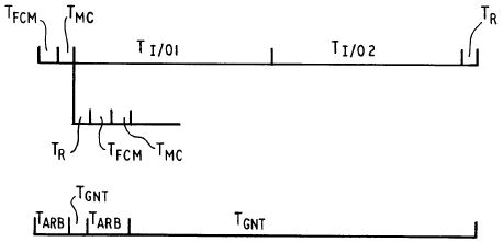
Figure 6 shows a timing diagram resulting from successive write operations by the CPU 38 to an I/O device 28. As shown by the top line of Figure 6, the write transfer 5 begins with delays TFCM and TMC caused by the delay introduced by the frequency control module 44 (TFCM) and the memory controller 58 (TMC). TI/O1 represents the first write cycle of data from the CPU 38 to an I/O device 28 over the I/O bus 32 which is posted (buffered) in the translation logic 106. TI/O2 represents the second write cycle of write data over the I/O bus 32. TR is a ready signal provided to the CPU upon completion of the write activity on the I/O bus 32.
Because the first write cycle data is posted, a TR ready signal may be provided to the CPU immediately upon posting. Thus, the delays TFCM and TMC inherent with CPU communications through the frequency control module 44 and the memory controller 58 may occur over the system bus 76 simultaneously as the write cycle is completed over the I/O bus 32. The second write cycle TI/O2 may proceed over the I/O bus immediately following the first write cycle TI/O1 If the first write cycle data were not posted, the time required for the ready signal Tr and the delays TFCM and TMC would have to occur intermediate the first and second write cycles TI/O1 and TI/O2. This time would not be masked under the first write cycle TI/O1 as shown in the top line of Figure 6, and would result in longer completion times to complete subsequent CPU to I/O device write cycles. Additionally, TI/O1 and TI/O2 can be conversion cycles as defined by the conditions of Figure 7.
Figure 7 Conditions under which to post cycles.
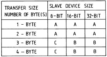
A. Cycle is posted
B. Cycle is posted if slave device has a 16 or 32 bit data bus width
C. Cycle is NOT posted
Posted write cycles and conversion cycles may occur simultaneously in the preferred embodiment of the present invention. The translation logic 106 is used as a buffer for both conversion and posted write operations. However, the conditions listed in Figure 7 must be imposed on the number of buffered cycles so as not to cause a system timeout. Refresh cycles occur only during a CACP arbitration mode, therefore, due to system memory requirements, and because a I/O devices 28 or CPU 38 may gain control of the bus just before the CACP is required to run a refresh cycle, the time between successive arbitration modes must not exceed 31.2 usec. As shown in Figures 5 and 6, the CACP circuit 62 does not enter arbitration mode intermediate subsequent I/O cycles of buffered data because the I/O bus activity is continuous and not interrupted by the handshaking delays TFCM and TMC. so Hence, the number of buffered 3.5 usec I/O cycles must be limited to ensure that 31.2 usec does not elapse intermediate successive arbitration cycles.
The handshaking delays occurring at the beginning of a posted write/conversion cycle (TFCM, TMC) account for approximately 0.2 usec. By buffering a maximum of six I/O cycles, under the conditions shown in Figure 7, CACP arbitration cycles will occur at least every [(6 x 3.5 usec) + (0.2 usec) = 21.2 usec]. Such a limit of six buffered I/O cycles allows for a minimum of 10.0 usec (31 .2 usec - 21 .2 usec) between the end of the last I/O cycle and the time at which a system timeout would occur due to failure to refresh system memory. This 10.0 usec minimum provides ample time for the DMA controller to enter arbitration mode, gain control of the system bus, and begin a refresh cycle. Accordingly, the preferred embodiment of a bus control logic system for computers having dual bus architecture has been described. With the foregoing description in mind, however, it is understood this description is made only by way of example, and that the invention is not limited to the particular embodiments described herein.