P&D-D (Plug and Display-Digital) Signal Pin Assignments - IEEE-1394
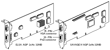
Digital (DVI) - Video (SVGA - combined) Card Samples

Pin
Signal
Pin
Signal
1
TMDS Data2 +
16
USB data +
2
TMDS Data2 -
17
USB data -
3
TMDS Data2 return
18
1394 outer shield (optional) &
Charge Power return 2)
4
Unused
19
1394 Vg
5
Unused
20
1394 Vp
6
Unused
21
TMDS Data0 +
7
TMDS Clock return
22
USB Data0 -
8
Charge power + 1)
23
TMDS Data0 return
9
1394 pair A, data -
24
Unused
10
1394 pair A, data +
25
DDC return
11
TMDS Data1 +
26
DDC data (SDA)
12
TMDS Data1 -
27
DDC clock (SCL)
13
TMDS Data1 return
28
+ 5 Vdc
14
TMDS Clock +
29
1394 pair B, Clock +
15
TMDS Clock -
30
1394 pair B, Clock -
Notes:
1) Optional output from monitor.
2) The IEEE-1394 internal cable bundle needs an outer shield to minimize internal crosstalk
within the cable construction.
The outer EMI containment shield for the IEEE-1394 function will be provided by the overall P&D cable shield.
If the internal bundle shield for IEEE-1394 is required, this may be terminated to pin # 18.
It is recommended that this implementation be evaluated in the case where both Charge Power return and the
IEEE-1394 internal cable bundle shield will be commoned to pin # 18.
TMDS = Transition Minimized Differential Signaling
Please see the LEGAL - Trademark notice.
Feel free - send a  for any BUG on this page found - Thank you.